
Nanoscience Instruments and our sister company, Nanoscience Analytical, provide cutting-edge instrumentation and process development services to enhance the production of medical devices and biomedical products…
Posted: September 6, 2023
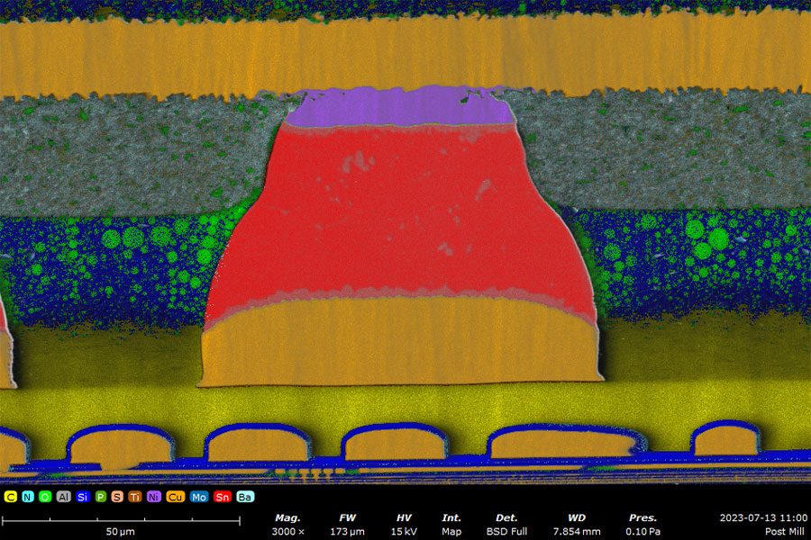
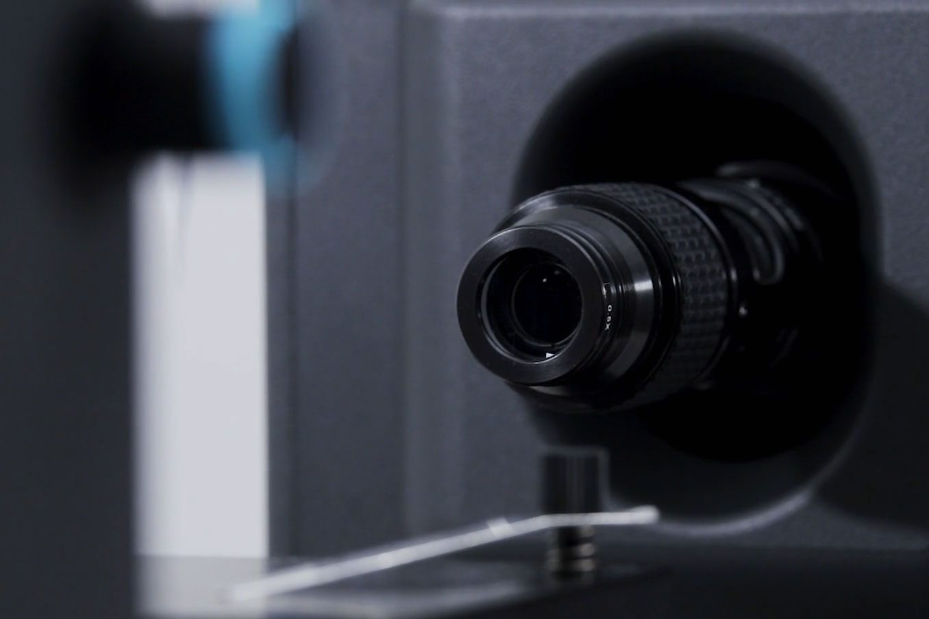
Failure analysis (FA) is an essential methodology that engineers use in the development process of semiconductor devices, like the CPU found in your smartphone or…
Posted: September 6, 2023
Scanning electron microscopy (SEM) is an incredibly adaptable analytical method that generates high-resolution images by scanning a focused electron beam across the surface of a…
Posted: August 30, 2023
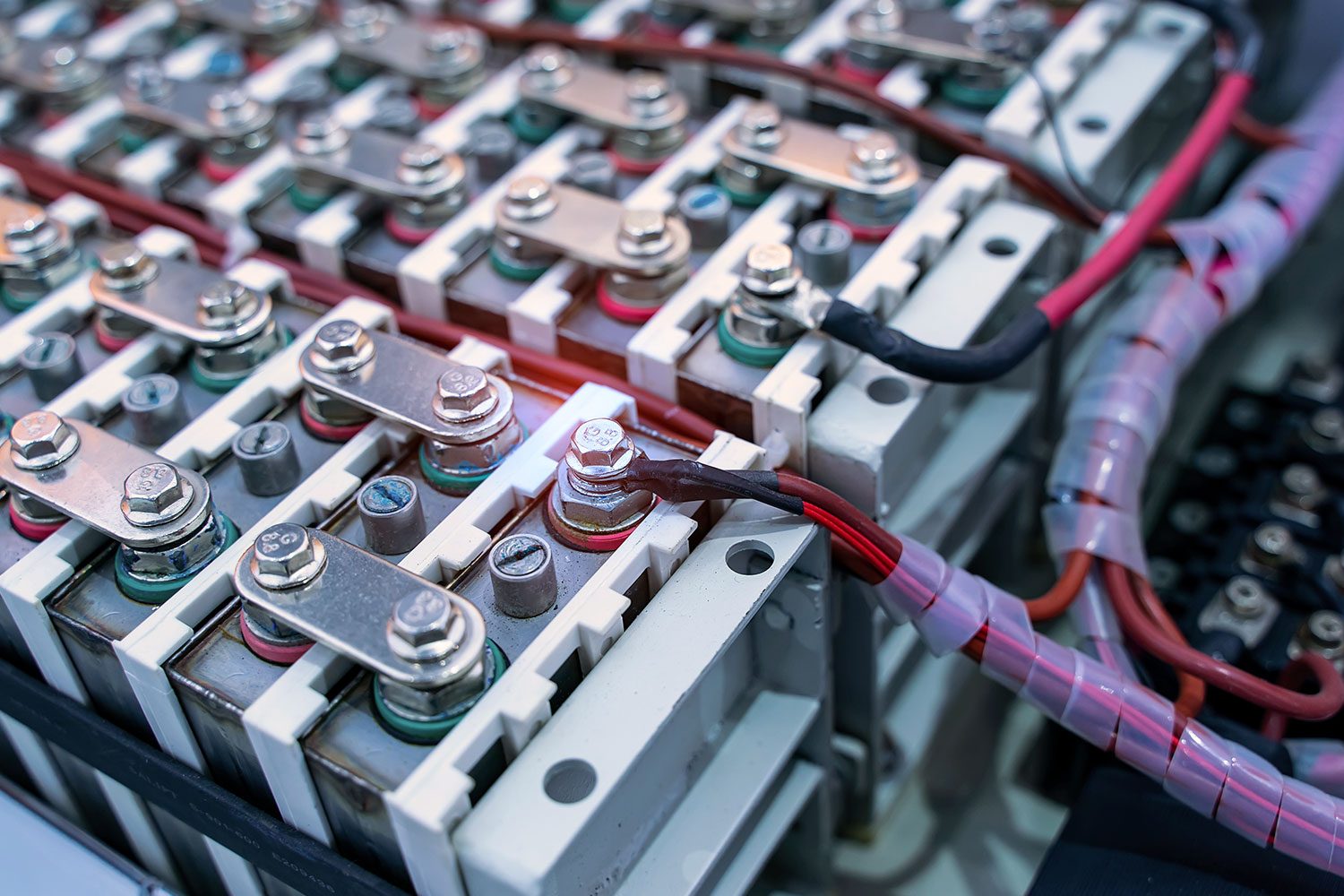
Battery testing is a crucial process in the development, manufacturing, and maintenance of various types of batteries. They play a vital role in powering a…
Posted: August 23, 2023

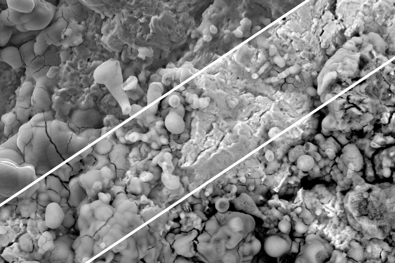
Imagine being able to visually explore the nanoscale structures of bugs, pollen, cells, minerals, and more. To zoom thousands of times closer than the naked…
Posted: August 16, 2023

Nanoscience Instruments cultivates global partnerships to deliver cutting-edge electron microscopy, surface analysis, and material characterization solutions. Visit our booth for live, hands-on demonstrations of industry…
Posted: August 11, 2023
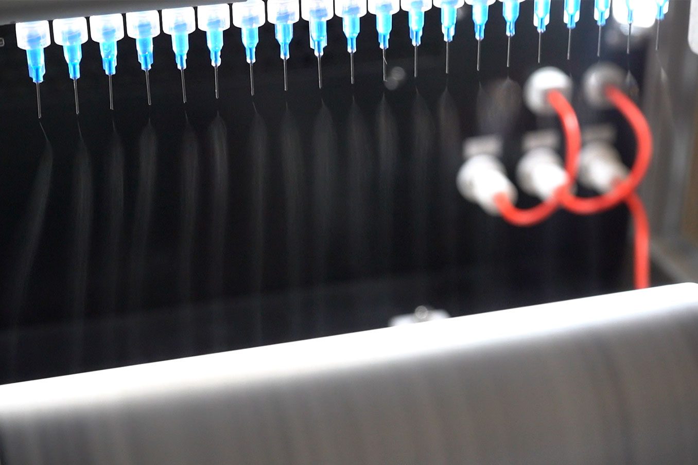
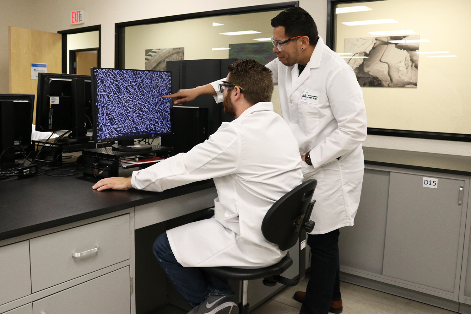
Electrospinning is a voltage-driven material fabrication process that can be used to produce micro to nano-scale fibers. The electrospinning process is a combination of interacting…
Posted: August 9, 2023

Nanoscience Instruments provides solutions for battery development applications through cutting-edge instrumentation and analytical services. Visit our booth for live demonstrations of desktop SEM with automated…
Posted: August 4, 2023
An optical tensiometer, also known as a contact angle goniometer, is an instrument used to characterize material surface properties and interactions between liquid and solid…
Posted: August 3, 2023
Scanning electron microscopy (SEM) is a technique that employs a focused beam of electrons to scan a surface, point by point, to examine a sample’s…
Posted: July 19, 2023
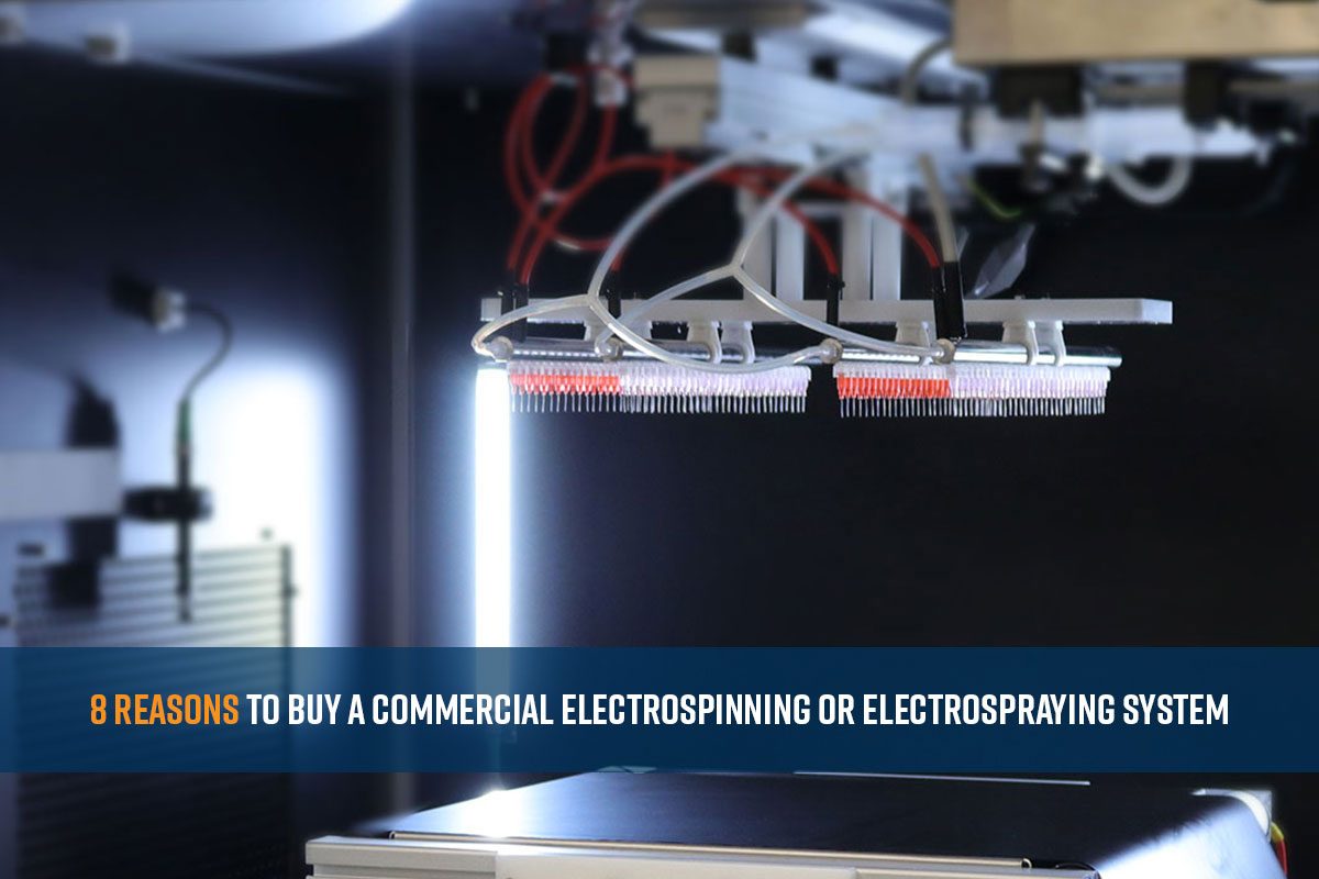
Electrospinning and electrospraying are electrohydrodynamic processes wherein a polymer solution is used to fabricate fibers or particles, respectively. In the most basic setup, a polymer…
Posted: July 17, 2023
In the domain of scientific research and advanced industrial applications, the scanning electron microscope (SEM) is a powerful tool that has revolutionized our understanding of…
Posted: July 12, 2023
Copyright 2024. Nanoscience Instruments. All Rights Reserved.
This site is protected by reCAPTCHA and the Google Privacy Policy and Terms of Service apply.