What is ChemiSEM?
In a scanning electron microscope (SEM) with Energy Dispersive X-ray Spectroscopy (EDS), a sample’s elemental composition is identified via the X-rays emitted during the electron beam interactions. Typically, acquiring compositional data involves a multi-step process. The SEM image is captured first and subsequently EDS data is collected by either map, spot, region, or line analysis. This process entails setting up ideal acquisition parameters, beginning the data collection process, and waiting to collect sufficient EDS signal.
ChemiSEM continuously collects quantitative elemental data during SEM imaging and overlays it on the morphological data in real-time, thereby eliminating the numerous steps in a typical workflow. With ChemiSEM, the elemental composition data of the sample is visualized as color-coded and wholly integrated in the SEM image. ChemiSEM is available on all Phenom Desktop SEM’s.

How Does ChemiSEM Work?
ChemiSEM uses a combination of machine learning and ultrafast signal processing to provide elemental maps in real time over a live SEM image. As the electron beam scans the sample, X-ray data is continuously collected and processed, providing instant visual feedback on the sample’s elemental composition. Background quantification of the signals provides a live map of the sample’s composition, displaying a live image of pixel-by-pixel elemental analyses simultaneously. This makes elemental analysis more accessible and faster than ever before. Users have multiple options with how much coloration is applied, which elements to include or exclude, and they can also use a spot analysis tool to check weight or atomic percentage on any given feature.
Advantages of ChemiSEM
ChemiSEM is a powerful feature of the Phenom Desktop SEMs that integrates SEM and EDS functionalities into a single, cohesive platform. This integration simplifies workflows, reduces analysis time, and enhances the accuracy of data interpretation. ChemiSEM offers a quick window into the elemental makeup of a sample where users can navigate to a color-coded area of interest where the contaminant may be and investigate further with a single click.
Real-Time Elemental Analysis
ChemiSEM provides live access, during SEM imaging, to quantitative elemental information that is displayed as color-coded overlays on SEM images. This allows for immediate identification of elemental composition and distribution.
Simplified, User-Friendly Workflow
The integration of SEM and EDS into one step eliminates the need for separate analysis steps, reducing complexity and saving time.
Accurate Data Processing
Elemental data is more precise and reliable with advanced algorithms to remove common artifacts and handle peak overlaps.
Shadow Removal
ChemiSEM’s advanced algorithm can provide a full elemental map without worrying about the shadow regions of non-flat samples.
Phase Mapping
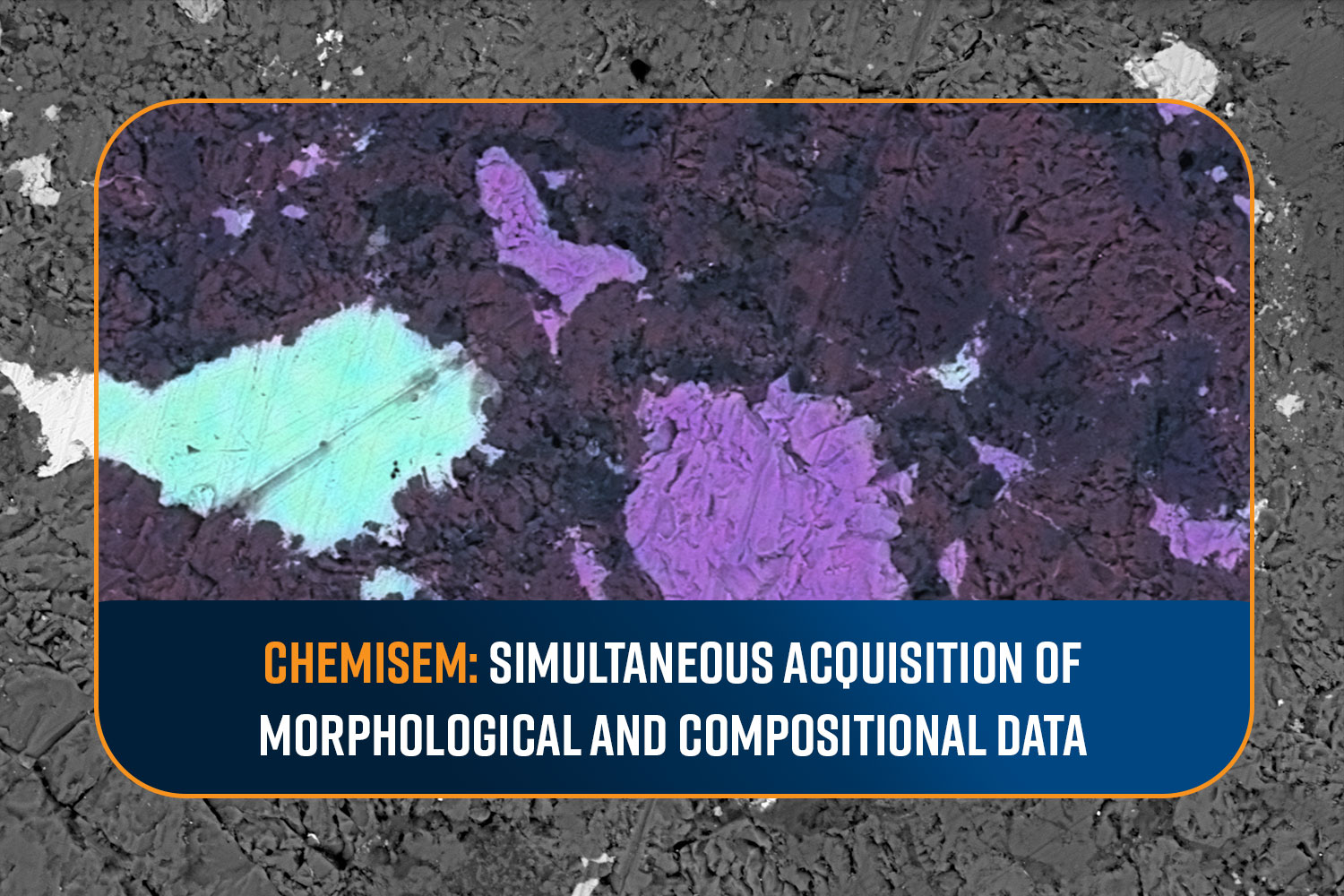
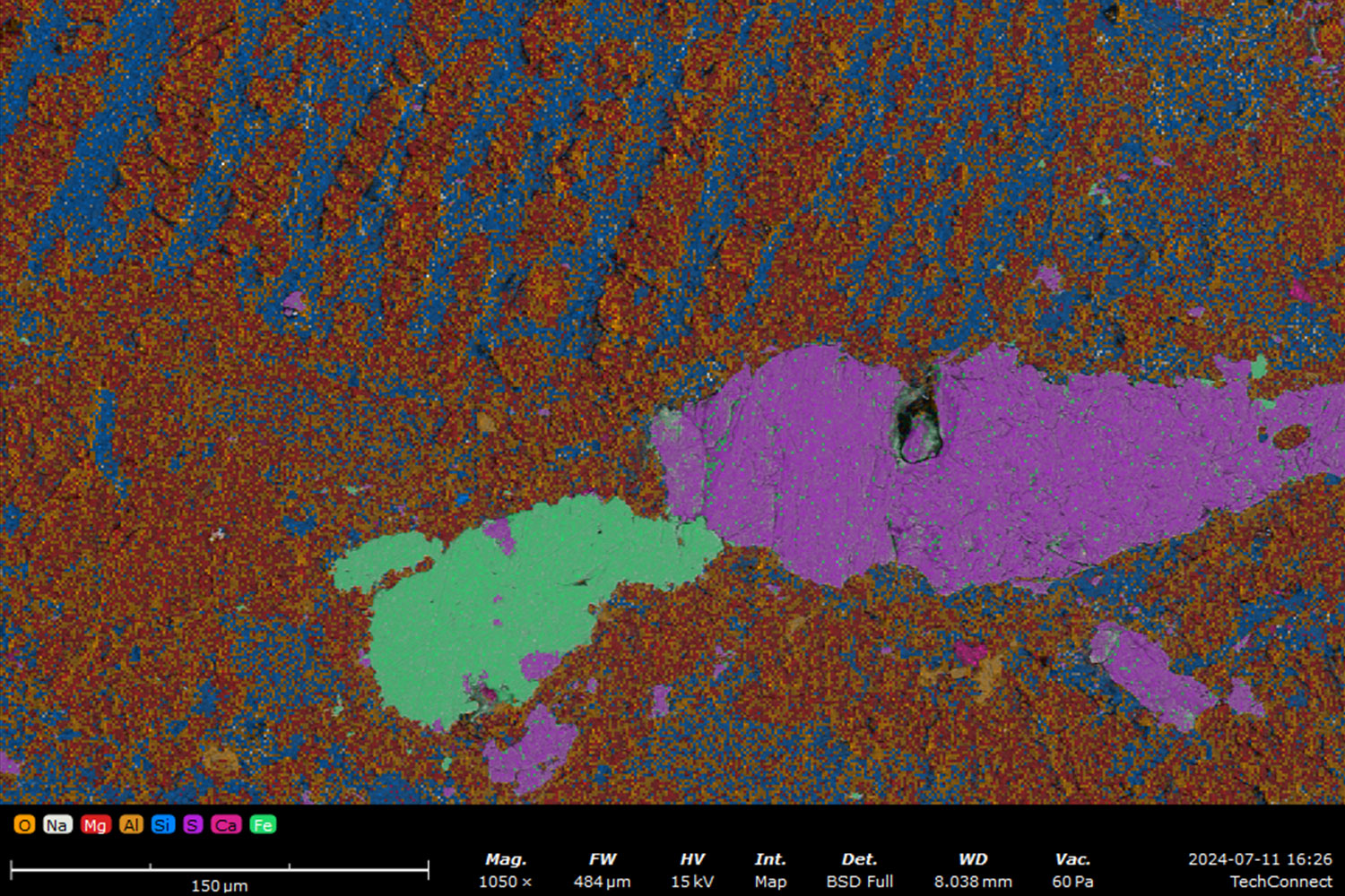
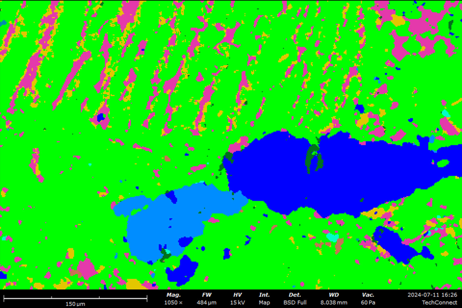
ChemiPhase is a feature of ChemiSEM that delivers precise phase mapping using principal component analysis (PCA)-based techniques. When acquiring an elemental map of multiphase materials, it may be difficult to interpret the map and clearly see where certain phases are located. When using ChemiPhase, the pixels are grouped based on the similarity of the spectral data (Figure 1). This allows for the data interpretation to be unbiased and allows for clear identification of distinct material phases with pixel-level accuracy, making it highly useful for research in composite materials, metallurgy (like steel inclusions), and geology.
What are Some Common Applications?
Material Science
In materials science, while analyzing a composite material, morphological data is combined with EDS data to immediately see the distribution of different elements within the sample.1 In quality control, a technician inspecting a manufactured component can identify contaminants and their compositions without switching to any other part of the UI.
Contamination of Battery Materials
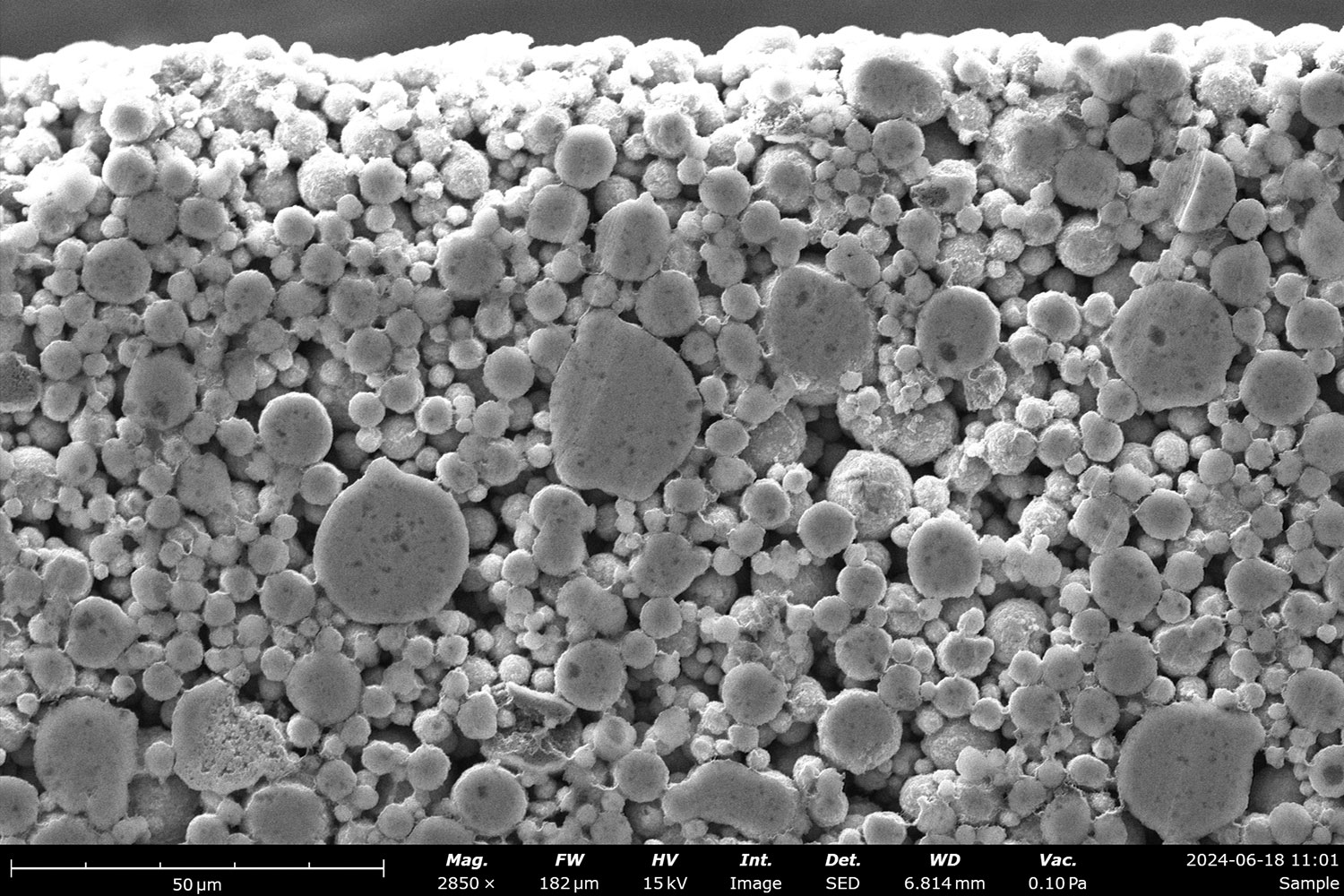
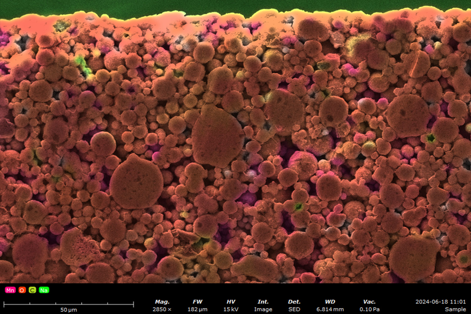
Contamination in battery materials can severely affect performance.2 Often, very low levels of contaminants need to be detected and standard EDS analysis can be a slow and time-consuming process. In analyses of battery material analysis (electrodes, NCM powders, etc.), ChemiSEM provides near-instant access to quantitative elemental information, allowing researchers to quickly identify contaminants and their sources (Figure 2).
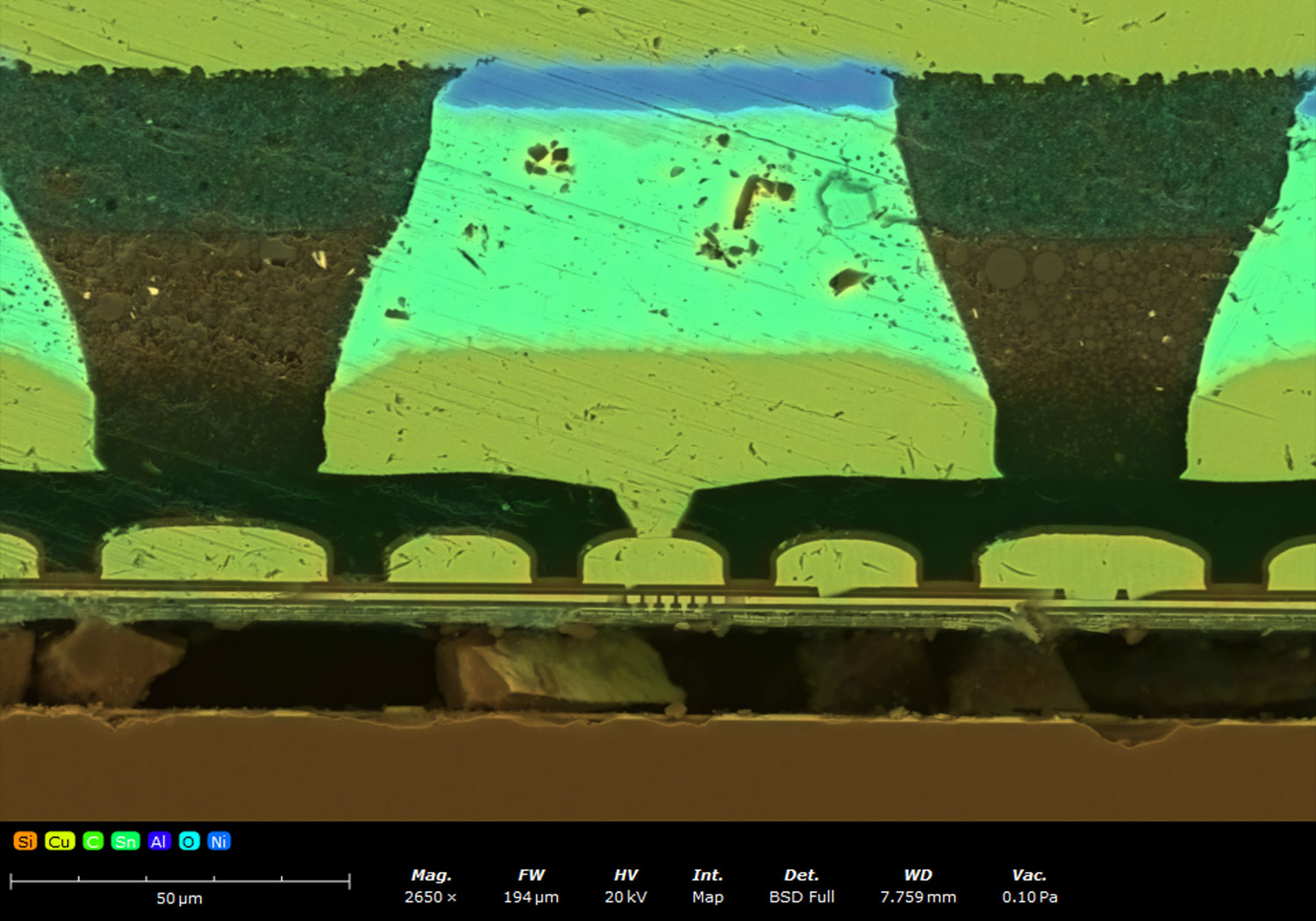
Failure Analysis and Quality Control
In failure analysis and quality control, the ability to simultaneously acquire SEM and EDS data is highly valuable. Traditional workflows involve capturing SEM images, then performing separate EDS analyses to identify the elemental composition of different components, whether it be a spot analysis or an entire elemental abundance map. These maps may take some time to collect, but ChemiSEM gives users a quick look at chemically different areas during imaging so that areas of interest can be further analyzed (Figure 3).
Conclusion
In summary, ChemiSEM provides real-time elemental analysis during SEM imaging, merging simplified and efficient chemical composition analysis with high resolution imaging. ChemiSEM stands apart as a unique solution with its accurate data processing for artifact removal and a user-friendly interface accessible to all skill levels. These features enhance applications in failure analysis, quality control, and contaminant analysis.
References
- Ali, A.; Zhang, N.; Santos, R.M. Mineral Characterization Using Scanning Electron Microscopy (SEM): A Review of the Fundamentals, Advancements, and Research Directions. Appl. Sci. 2023, 13, 12600. https://doi.org/10.3390/app132312600 ↩︎
- Jiacheng Zhu, Xuefeng Wang. Electron Microscopy for Advanced Battery Research. Microscopy and Microanalysis for Lithium-Ion Batteries. 2023, 1st edition. 478. https://doi.org/10.1201/9781003299295 ↩︎