Scanning Electron Microscopy (SEM) is a powerful imaging technique that allows for the observation of the surface details of a sample at very high magnifications. One of the key parameters in SEM imaging is the accelerating voltage, which plays a crucial role in determining the quality and type of information that can be obtained from the sample. In this blog, we’ll explore the significance of accelerating voltage in SEM imaging, covering how it affects resolution, surface sensitivity, contrast, as well as practical considerations when dealing with different types of samples.

Understanding Accelerating Voltage
Accelerating voltage refers to the potential difference that accelerates electrons from the electron gun down the column and toward the sample in an SEM. This voltage is typically measured in kilovolts (kV) and usually ranges from 1 – 30 kV. The chosen accelerating voltage impacts the energy of the beam’s electrons, which affects their interaction with the sample.
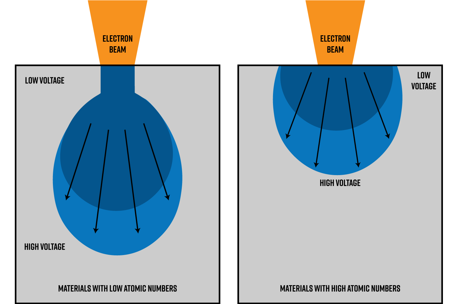
An important concept to understand when thinking about accelerating voltage is the volume of interaction. When the electron beam strikes the sample, electrons penetrate the sample surface and interact with constituent atoms, defined as the interaction volume. The size and shape of the interaction volume depends on the accelerating voltage of the electron beam and the material properties of the sample (Figure 1).1 Higher beam energies generally result in larger interaction volumes, while lower beam energies produce smaller, more surface-confined interaction volumes. Samples composed of light elements (like polymers or biological matter) result in larger interaction volumes compared to denser materials (like metals or ceramics). Typically, accelerating voltage is chosen based on the sample to optimize resolution, surface sensitivity, and minimize potential damage to the sample
Effects on Image Resolution
In SEM, resolution is defined as the ability to distinguish between two closely spaced points on the sample. It is a measure of the microscope’s capability to reveal fine detail and is typically expressed in nanometers (nm). Higher resolution means that features spaced close to one another can be distinguished and imaged clearly.
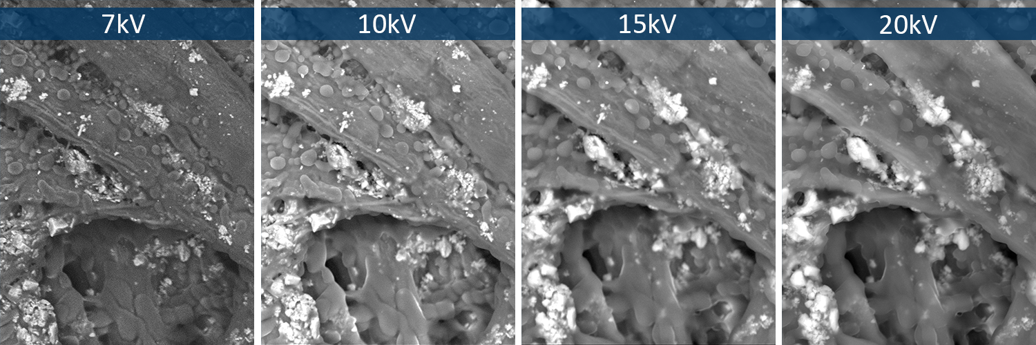
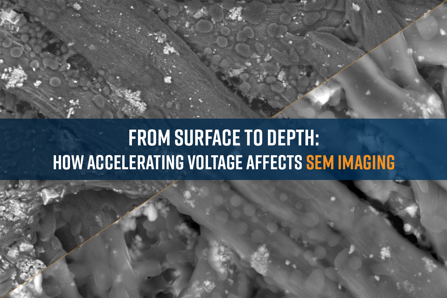
Accelerating voltage has a major impact on resolution through its effect on the interaction volume. Higher voltages can penetrate deeper into the sample, increasing the interaction volume and potentially decreasing resolution (Figure 2). Lower voltages reduce the interaction volume and improve surface resolution. However, using too low of an accelerating voltage can result in a low signal-to-noise ratio (SNR), thereby degrading resolution. Therefore, the accelerating voltage must be optimized to balance these competing effects.
The type of electron source also impacts how the resolution varies at different accelerating voltages. For thermionic emission sources, such as a CeB6-based electron gun found in the Phenom XL Desktop SEM, the optimal accelerating voltage is about 10 kV. On the other hand, field-emission SEMs, like the Phenom Pharos Desktop SEM, can maintain smaller spot sizes at higher accelerating voltages leading to better resolving capabilities even at high accelerating voltages.
Surface Sensitivity
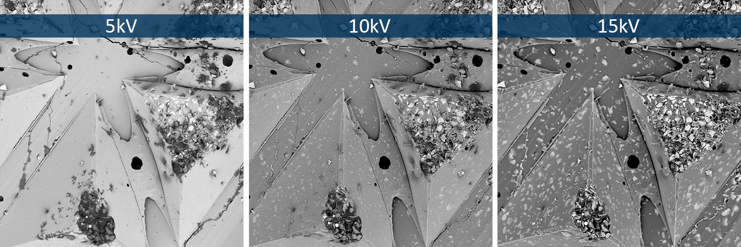
Understanding surface sensitivity in SEM imaging is important for accurately interpreting images and adjusting imaging conditions to meet specific needs. At higher accelerating voltages, electrons penetrate deeper into the sample, generating more secondary electrons (SEs), backscattered electrons (BSEs), and characteristic X-rays, which are crucial for imaging and analytical techniques such as Energy Dispersive X-ray Spectroscopy (EDS). This deeper penetration can be beneficial for analyzing the internal structure of a sample or for thicker specimens.
Lower accelerating voltages, however, limit electron penetration to the near-surface region, which is advantageous for observing fine surface details and delicate samples that may be damaged by higher energies (Figure 3). This shallow interaction is particularly useful for materials like biological specimens or polymers, which can be easily damaged by high-energy electrons.
Effects on Image Contrast
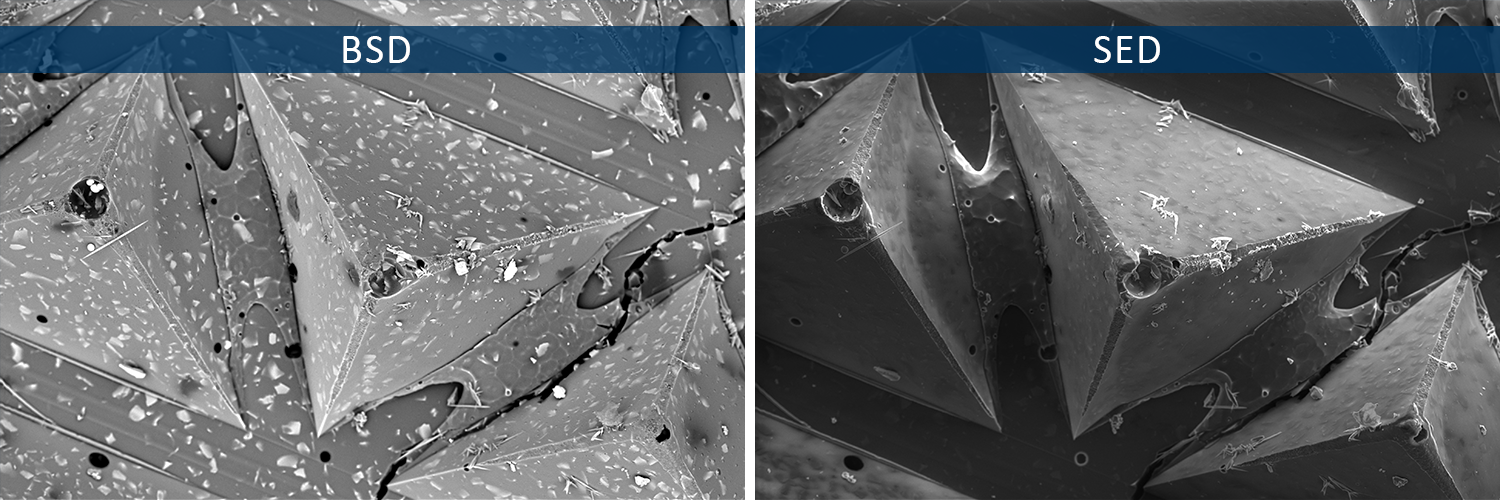
Accelerating voltage can impact SEM image contrast (Figure 4) through different mechanisms:
- Material and phase contrast: BSE imaging mode is useful for visualizing a material’s microstructure since image contrast is dependent on average atomic number. Heavier elements have higher BSE yield and therefore produce a brighter signal compared to regions containing lighter elements. Since higher accelerating voltages increase the penetration depth of electrons into the sample, more BSEs can be generated. This effect can increase the contrast between areas of different atomic number because heavier elements backscatter more electrons.
- Topographic contrast: SE imaging mode is used for topographic imaging because SEs uniformly escape from the surface, unlike BSE emission which depends upon the local atomic number. Lower accelerating voltages can enhance topographic contrast and edge effects because the electrons interact more with the sample surface, highlighting surface irregularities and edges.2
Practical Considerations and Applications
Accelerating voltage |
Goal |
Applications |
||
| 1-5 kV | Preserve the integrity of delicate structures and enhance surface detail. |
|
||
| 5-10 kV | Achieve a good balance between resolution and surface sensitivity for most materials. |
|
||
| 10-30 kV | To probe deeper into the material and to obtain compositional information. |
|
||
Table 1: General guideline for selecting the appropriate accelerating voltage.
Selecting the appropriate accelerating voltage for SEM imaging requires a balance between resolution, surface sensitivity, contrast, and the specific requirements of the sample being studied. Table 1 is a general guideline for selecting the right accelerating voltage for CeB6-based SEMs, like the Phenom XL, ProX, Pro, and Pure Desktop SEM models.
Conclusion
The accelerating voltage in SEM imaging is a critical parameter that significantly impacts the resolution, contrast, and interaction of electrons with the sample. By carefully selecting the appropriate accelerating voltage, researchers can optimize their imaging conditions to obtain the best possible information from their samples. Understanding the effects of accelerating voltage helps in tailoring SEM techniques to the specific needs of various scientific and industrial applications, ultimately enhancing the power and versatility of this indispensable imaging tool.