Automated Multi-modal Acquisition & Visualization Software
Maps for Phenom Desktop SEM
Introducing Maps software, a powerful enhancement for Phenom Desktop Scanning Electron Microscopes (SEMs), crafted to elevate the efficiency and depth of your analytical workflows. Maps software automates acquisition of large datasets, including SEM imaging and EDS mapping, and seamlessly stiches and aligns them to provide detailed visualization across expansive sample areas.
High-Resolution, Large Area Imaging & EDS Maps
Capture and seamlessly stitch expansive, high-resolution SEM images and EDS maps, enabling fast, detailed exploration of your samples.
Effortless Automation
Automate imaging sessions with unattended operation, maximizing microscope efficiency and ensuring high-quality data with minimal oversight.
Integrated Correlative Microscopy
Align and overlay data acquired from different instruments for cohesive, multi-modal insights into your samples.
Talk to an Instrumentation Specialist Today!
Maps for Phenom
Software Features
Beyond enhancing the Phenom’s capabilities, the Maps UI is compatible across Thermo Scientific microscopes including SEM, FIB-SEM, TEM, and XPS systems, providing guided workflows for acquiring and analyzing correlated datasets.
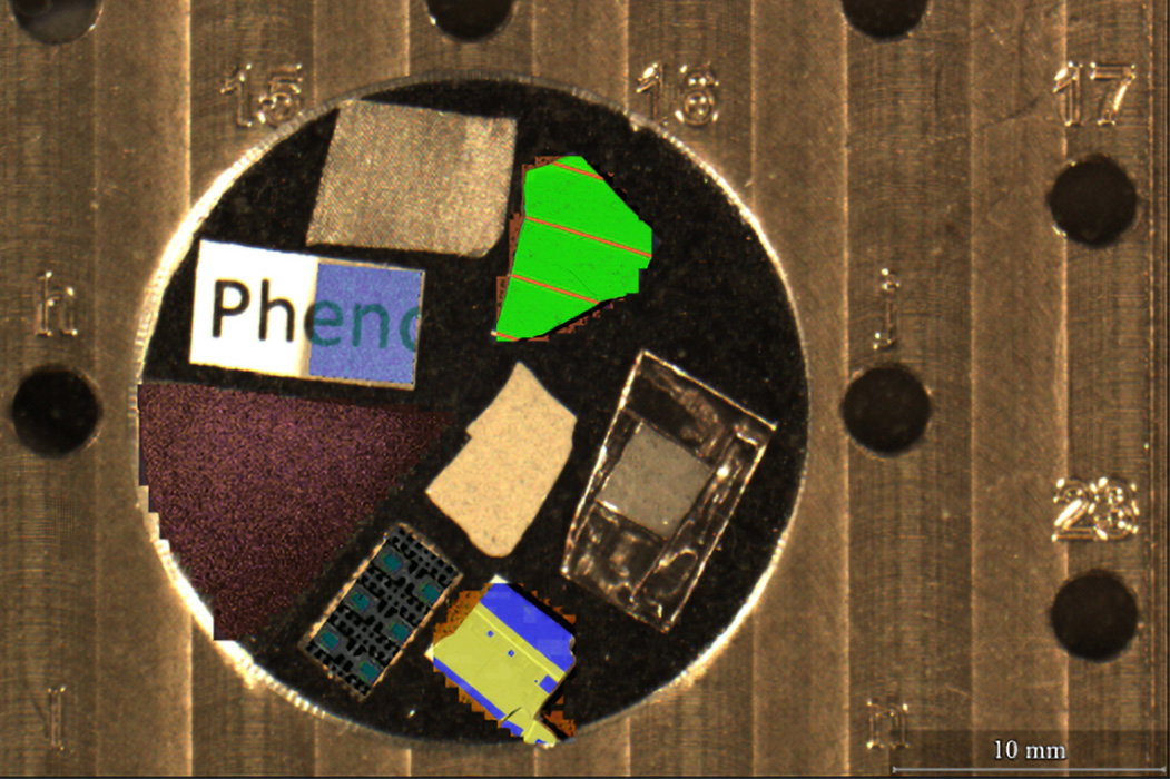
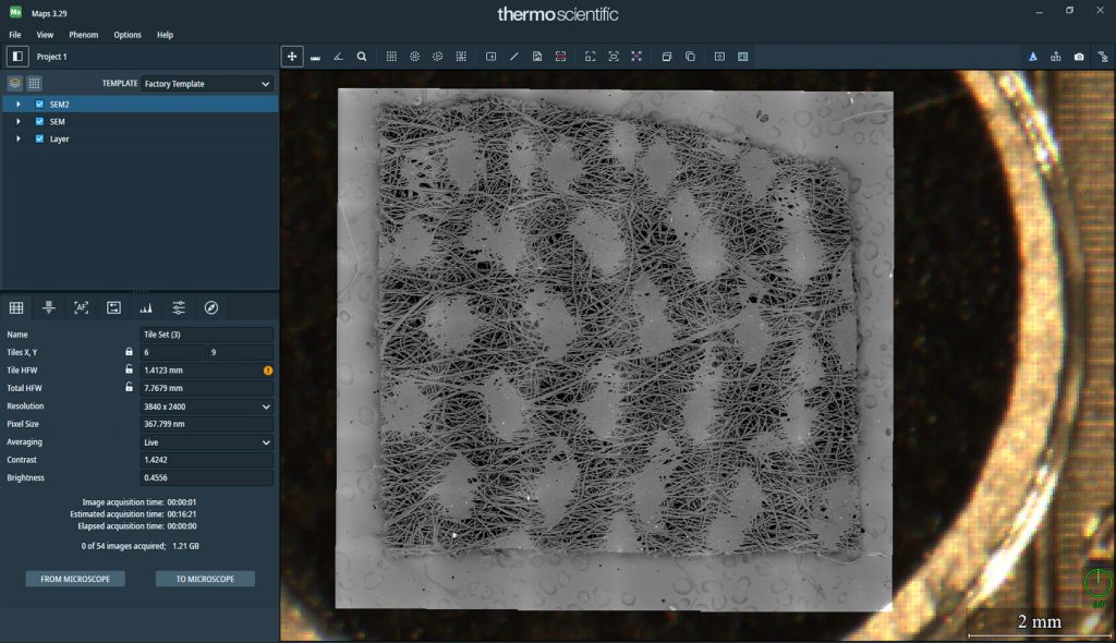
Tile Set Acquisition
Tile sets are arrays of individual images (or EDS maps) that systematically cover a defined sample area. With the tile set acquisition panel in Maps, users can customize key parameters—such as the number of tiles, resolution, and frame averaging—to suit their specific analysis needs. Estimated acquisition times for each tile and the complete tile set are displayed upfront, allowing you to plan and optimize your workflow for maximum efficiency.
Unattended operation
Smart acquisition allows users to set up and run multiple tile sets on various samples, enabling hands-free jobs that optimize microscope time without sacrificing data quality or quantity.
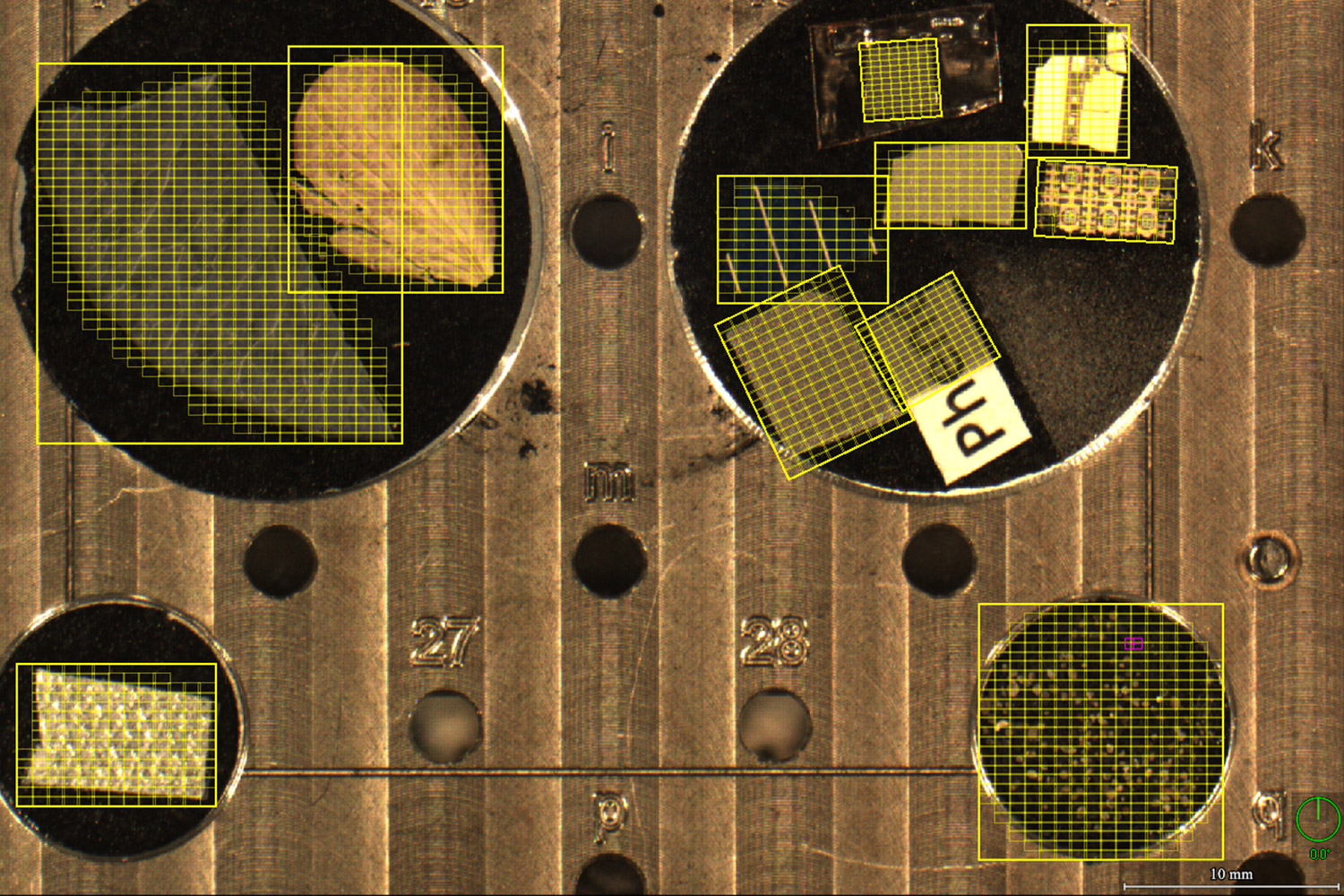
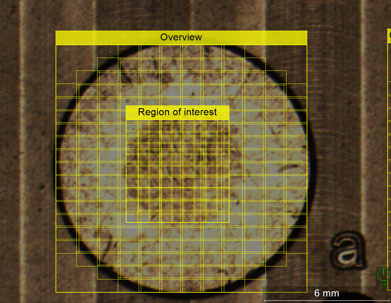
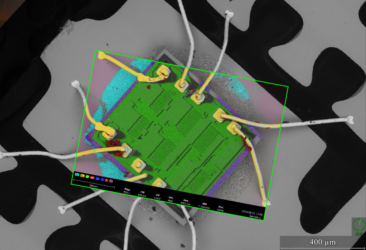
Large-area High Resolution Imaging
Save time searching for regions of interest during microscope sessions. Maps divides large areas into smaller tiles, stitching them together seamlessly to create a multi-scale image viewable at both low and high magnifications.
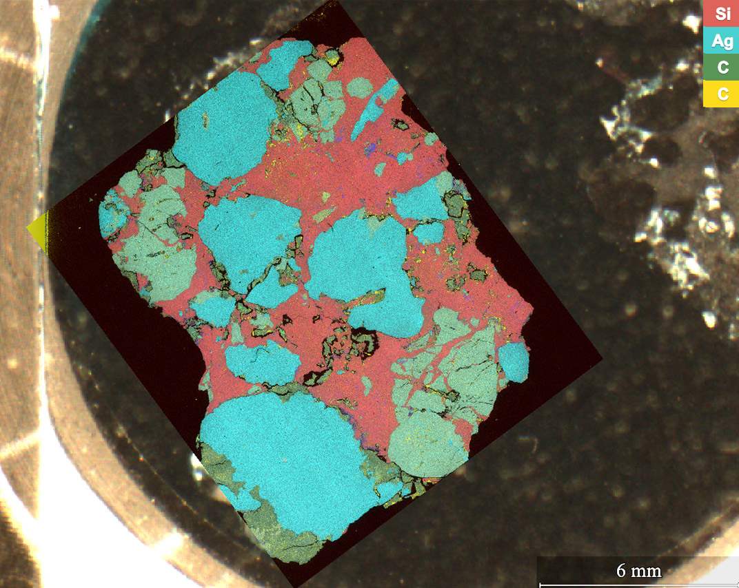
Compositional Overview of Sample
Maps can generate low-magnification elemental maps faster than traditional methods, allowing you to quickly visualize the distribution of elements across your entire sample. Additional elements can be added post-acquisition, with EDS mapping data accessible for each tile within the intuitive Phenom UI.
Correlative Data Workflows
MAPS offers a consistent UI across Thermo Fisher microscopy equipment, including SEM, dual-beam FIB-SEM, TEM, and XPS systems. Guided workflows allow users to acquire data from the same area of interest, enabling seamless multi-modal, correlative datasets.
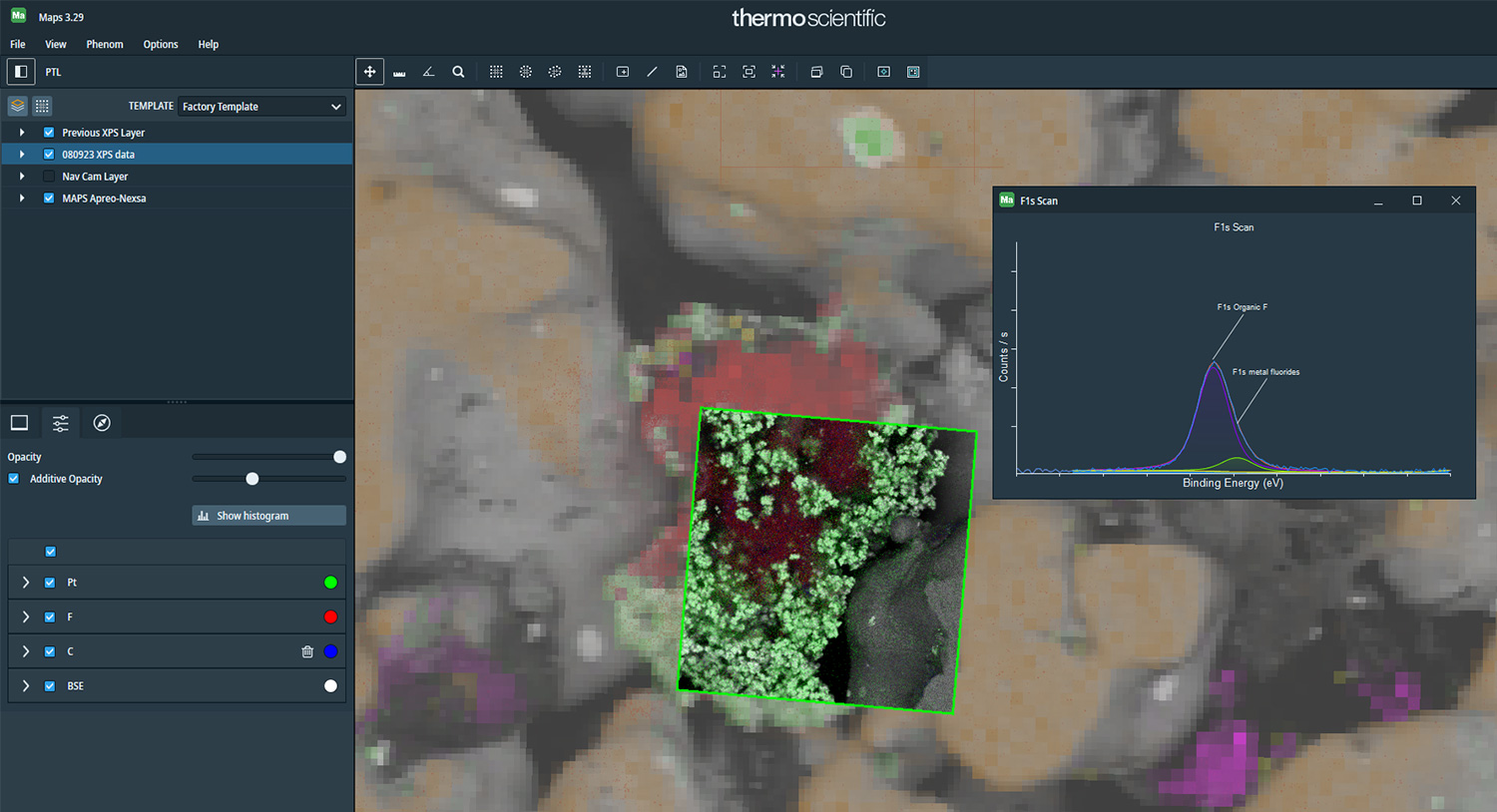
Data Management and Offline Analysis
The Maps offline viewer provides an environment to dive deeper into your data. Import data from various sources – from the optical navigation camera, electron microscope images, EDS maps, Phase maps, and spectral images containing XPS, Raman, and IR data – and easily align and organize overlays for detailed visualizations.
MAPS for Phenom
Product Knowledgebase
Using Automated SEM/EDS Analysis to Enhance Parts Cleanliness
Maintaining technical cleanliness is critical in industries where contamination can compro…

5 Benefits of Scanning Electron Microscopy for Particle Analysis
Particle analysis is a critical process in many industries, from pharmaceutical formulatio…

Automated SEM/EDS Monitoring of Steel Inclusions for Compliance with ASTM Standards
In modern steel manufacturing, non-metallic inclusions represent a critical quality concer…