Materials scientists leverage a range of advanced analytical techniques to extract detailed information regarding a sample’s structure, properties, and defects. Scanning electron microscopy (SEM) is a cornerstone of these methods, offering critical insights into surface morphology and elemental distribution at the nanoscale. Among the many signals generated in SEM, backscattered electrons (BSEs) play a crucial role in providing compositional contrast and structural insights. By analyzing these high-energy electrons, which are reflected from the sample surface, researchers can uncover information about the distribution of elements, crystal orientations, and even surface topography. In this blog, we’ll explore the fundamentals of BSEs, the insights gained from BSE imaging, and how the Phenom Desktop SEM takes BSE imaging to the next level.

What are Backscatter Electrons?
BSEs are generated through elastic interactions between the electron beam and the sample. In simple terms, they are the original beam electrons that have been reflected out of the sample’s surface without losing much energy.
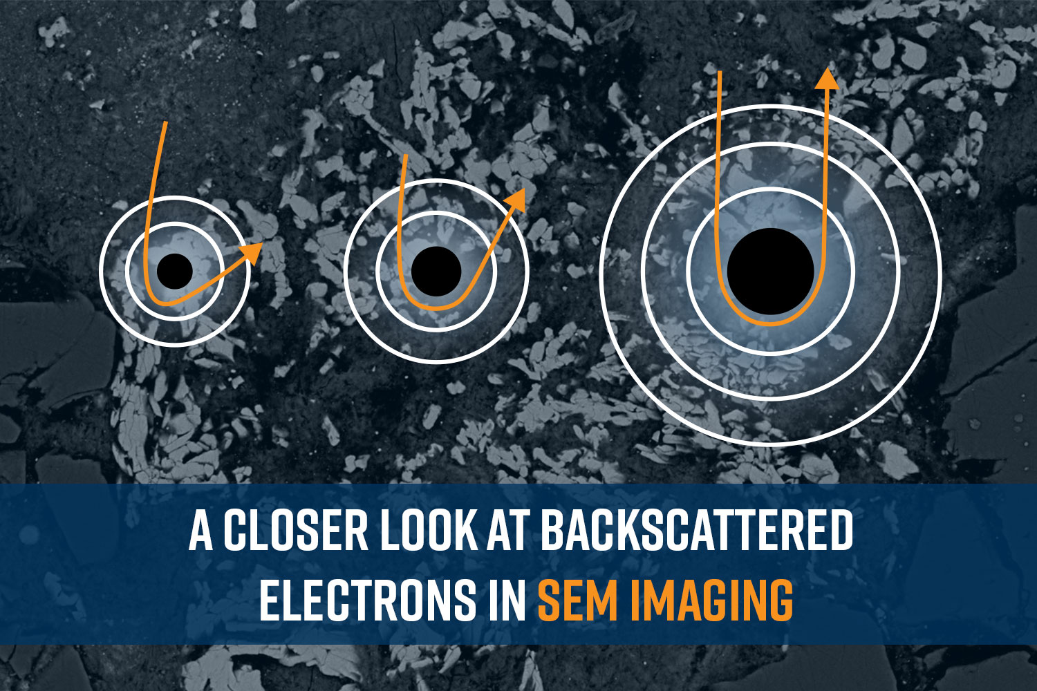
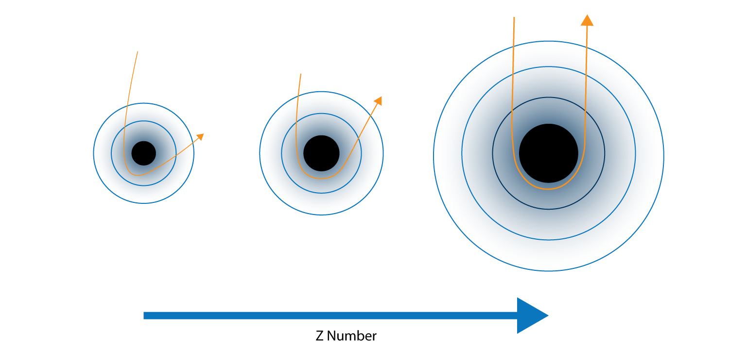
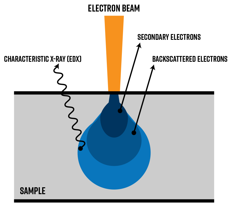
When an electron beam strikes the surface of a sample, these electrons penetrate below the surface and interact with the atoms in the material. The positively charged atomic nuclei create a Coulomb field that can change the path of the incoming negatively charged electrons. Heavier elements, which have nuclei with a higher atomic number, are more likely to deflect the electrons at a higher angle, while lighter elements cause only slight deflections. Electrons that are deflected at high angles are more likely to escape the sample and be captured by the BSE detector (BSD) (Figure 1). This phenomenon is responsible for the elemental contrast observed in BSE images.
In a SEM, BSEs that originate from up to hundreds of nanometers below the sample surface can be detected. This depth is roughly ten times greater than that of the secondary electron signal, which results from inelastic scattering (Figure 2).
What can we Learn from BSE Images?
BSE images provide valuable information about a sample’s composition and structure. Some of the key insights that can be obtained from BSE images include:
- Microstructure: Since backscattered electrons are more likely to be reflected by heavier elements (those with a higher atomic number), areas containing such elements will appear brighter in the image. This contrast allows for the identification of different elemental distributions within a sample, providing a clear picture of its microstructure.
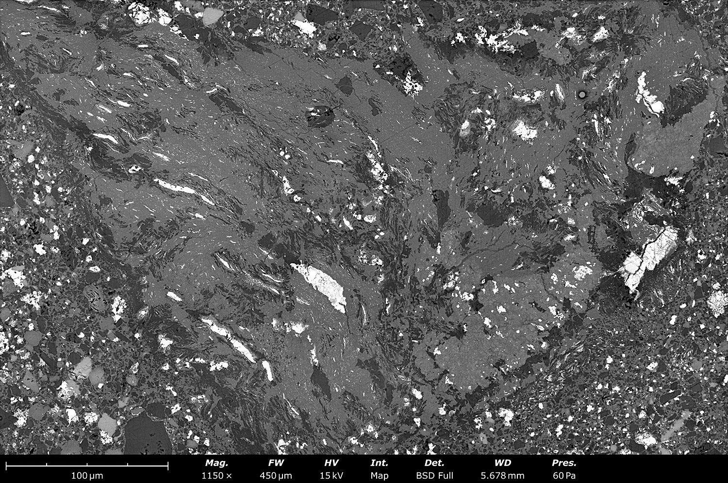
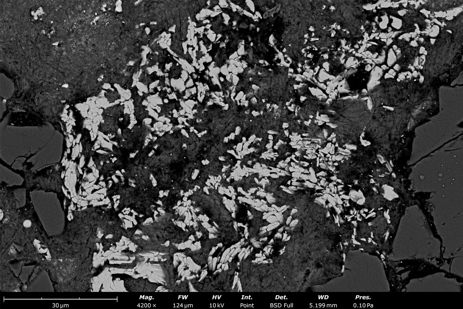
- Phase Identification: By analyzing the differences in brightness and contrast in BSE images, scientists can identify different phases within a multi-phase material. This is crucial in fields such as metallurgy, geology (Figure 3), and materials science, where materials often consist of various phases with distinct composition.
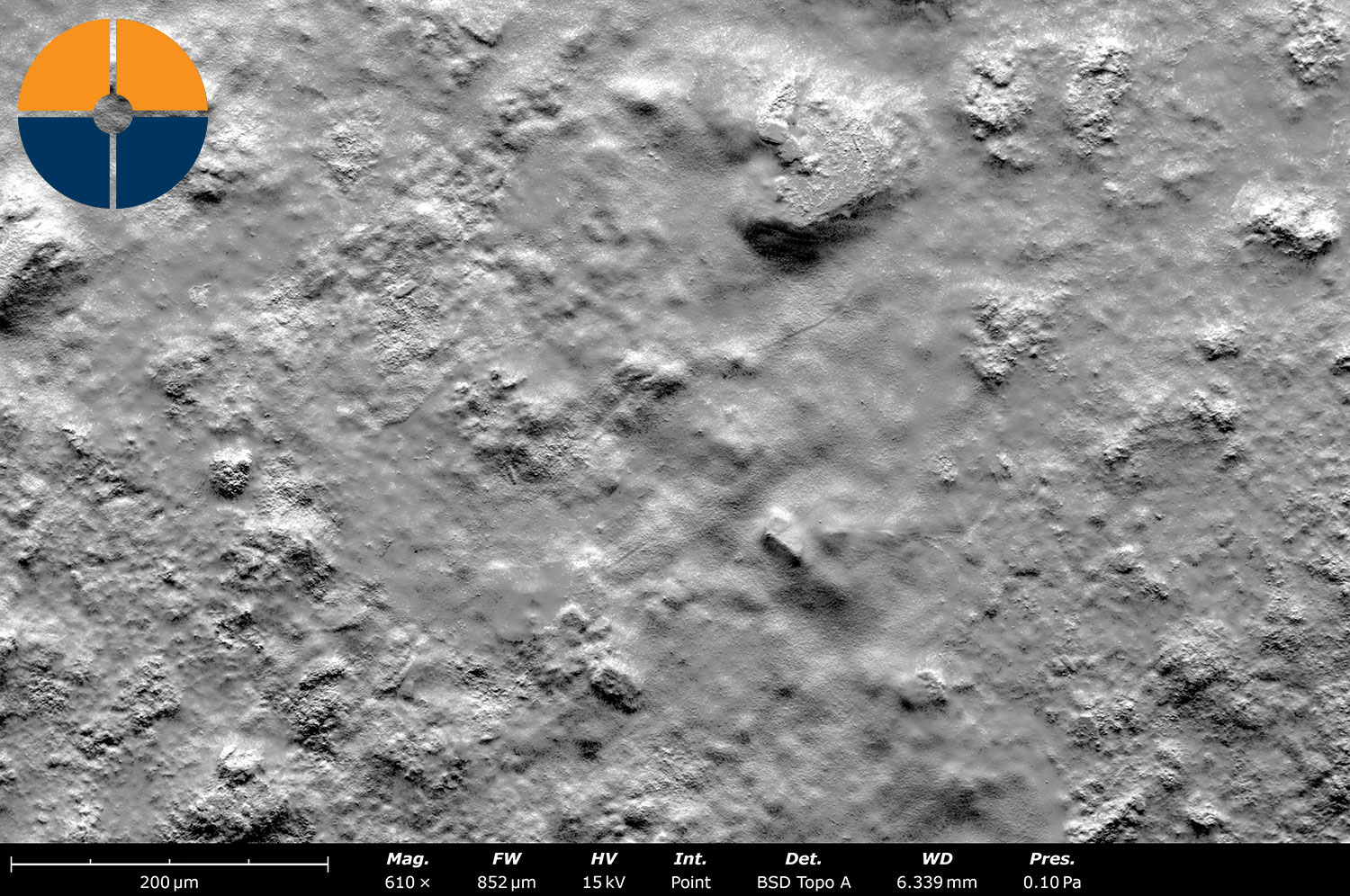
- Topographic imaging: In samples with topographic features, signal intensity varies based on the surface angle relative to the detector. Areas tilted toward the detector produce a stronger BSE signal and appear brighter, while those tilted away appear darker. Advanced software can process these signals to create a 3D model, offering both visual and quantitative information about the sample’s surface features.1
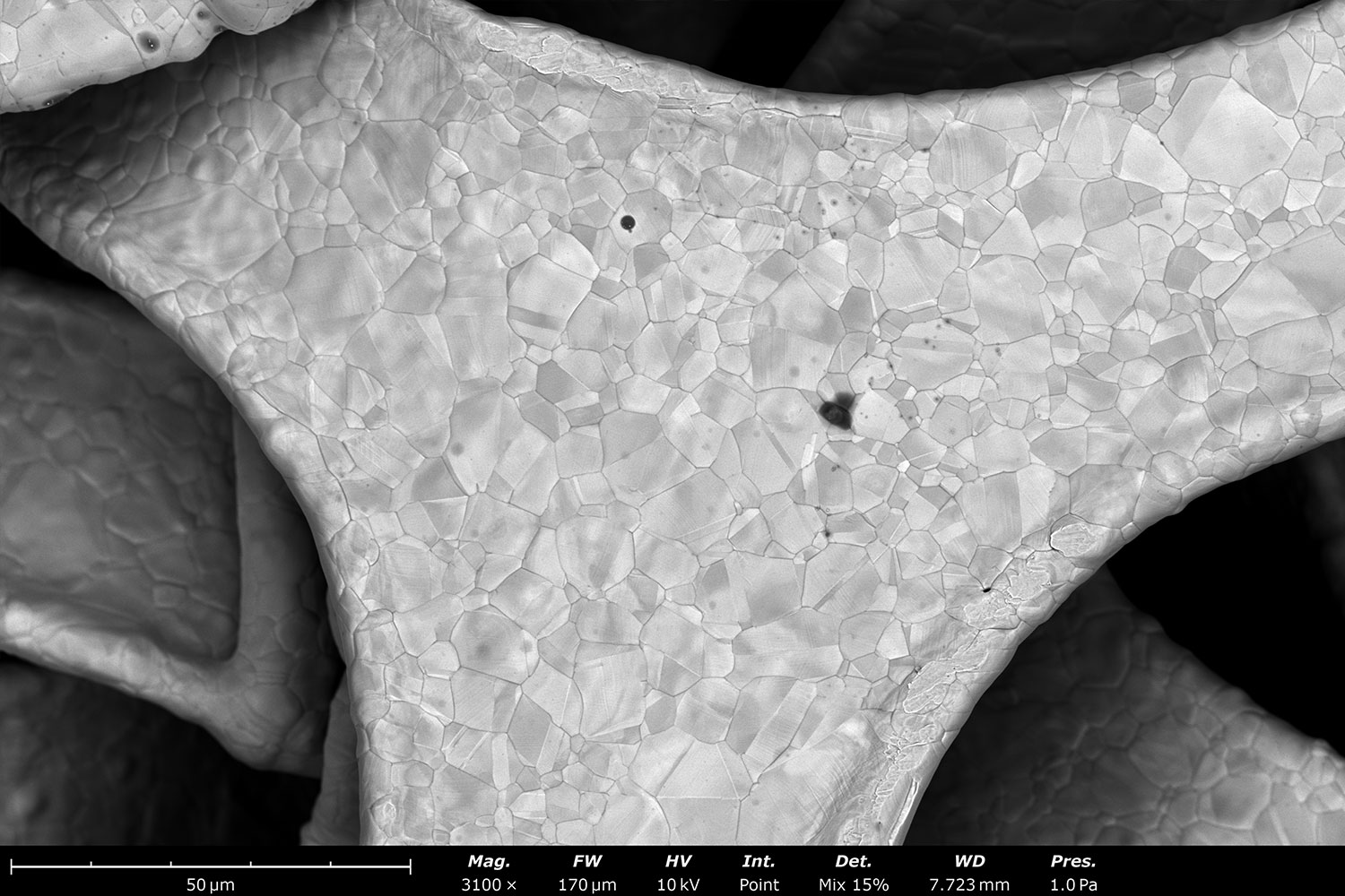
- Crystallographic Information: For samples with relatively large, distinct grains, BSE imaging can show variations in brightness corresponding to different orientations of these grains [2]. This is also known as channeling contrast imaging. The difference in backscatter efficiency due to the different orientations of the crystal planes relative to the electron beam direction can provide clues about the grain orientation and grain sizes (Figure 4).
BSE Imaging and Beyond with Phenom Desktop SEM
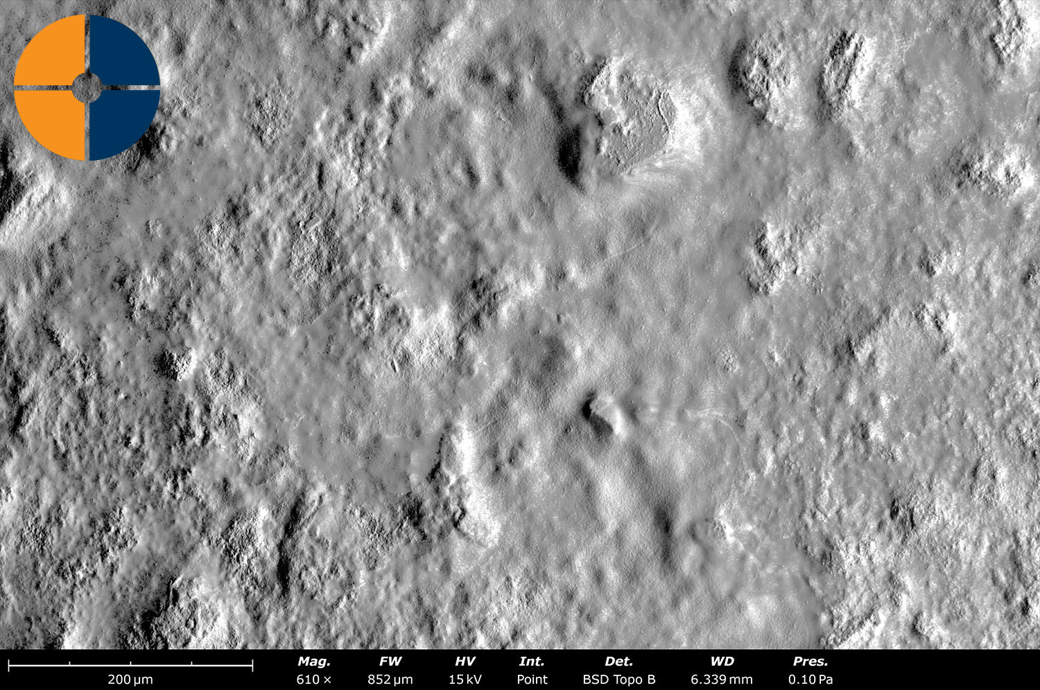
The Phenom Desktop SEM is a compact and user-friendly SEM designed to bring the power of electron microscopy to a broader range of users. All Phenom Desktop SEM models come standard with a segmented BSD (Figure 5), allowing for efficient BSE imaging and more advanced techniques like topographic mapping.
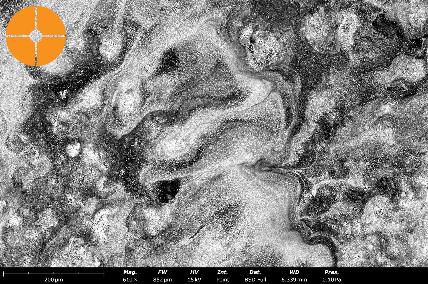
When all four quadrants are operated in tandem, the BSE detector maximizes signal collection efficiency for standard high-resolution imaging. Users also have the option to obtain topographic maps by using topographic imaging mode or the 3D Roughness Reconstruction (3DRR) application.
Topographic imaging modes, Topo A and Topo B, display the BSE signal difference between the upper/lower and left/right halves of the BSD (Figure 6). This allows for a qualitative interpretation of surface topography that may not be evident from BSE images alone.

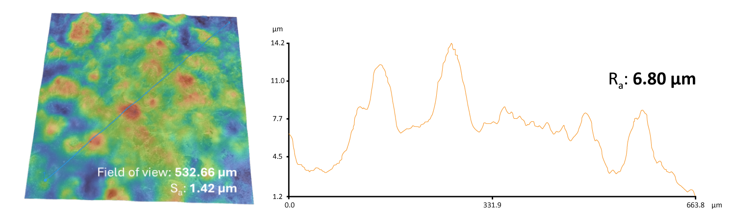
The 3DRR technique produces a 3D surface map, facilitating advanced interpretation and roughness measurements (Figure 7). Utilizing a “shape from shading” algorithm, the system calculates relative surface heights by analyzing signal variations across the four BSD quadrants.2 The data is presented as a heat map, offering clearer topographical insights than traditional grayscale images.
Key Takeaways
BSE imaging in SEM provides high-resolution visualization of a material’s elemental distribution and microstructure. Due to the sensitivity of BSEs to atomic number differences, they excel in highlighting compositional contrast, making them invaluable for analyzing complex, multi-phase materials. With a segmented BSD and advanced image processing software, SEM systems like the Phenom Desktop SEM enable the generation of 3D topographical maps. These maps not only offer qualitative insights into surface morphology but also support quantitative analysis of surface features, such as roughness and texture. Equipped with a highly efficient BSD, the Phenom Desktop SEM streamlines both compositional and topographical analysis, offering a powerful, accessible tool for comprehensive material characterization.
References
- . Hemmleb, D. Bettge, I. Driehorst and D. Berger, “3D surface reconstruction with segmented BSE detector: New improvements and application for fracture analysis in SEM,” in European Microscopy Congress 2016: Proceedings, 2016. https://doi.org/10.1002/9783527808465.EMC2016.6175 ↩︎
- M. A. Crimp, “Scanning Electron Microscopy Imaging of Dislocations in Bulk Materials, Using Electron Channeling Contrast,” Microscopy Research and Technique, vol. 69, pp. 374-381, 2006. https://doi.org/10.1002/jemt.20293 ↩︎