Introduction
Scanning electron microscopy (SEM) is a powerful instrument to examine the surface morphology and topography of materials at high magnification. Since SEM is inherently a 2D analysis technique, investigating layered or complex structures requires cross sectioning the sample. Cross-sectional analysis extends the SEM’s capability by providing insights into the internal structure of materials. By imaging a cross-section of a sample, researchers can observe layers, interfaces, defects, and other features not visible on the surface.
Many materials and devices have layered or multilayered structures, such as integrated circuits, thin films, coatings, and composites. Cross-sectional analysis in SEM enables researchers to visualize these layers and study their thickness, uniformity, adhesion, and interfaces. This is crucial for quality control, process optimization, and performance improvement in various industries.
In semiconductor and electronics industries, cross-sectional analysis is essential for characterizing devices and components such as transistors, diodes, MEMS (Micro-Electro-Mechanical Systems), and sensors. SEM imaging of cross-sections provides valuable information about device structures, dimensions, alignment, doping profiles, and fabrication processes. By analyzing cross-sections of samples before and after specific treatments or processes (e.g., deposition, etching, annealing), researchers can evaluate the effects of these processes on material structure and properties. This information is valuable for optimizing manufacturing processes, improving product performance, and achieving desired material properties.
Cross-sectional analysis is essential for investigating the causes of material failures or defects. By imaging a cross-section of a failed component or material, researchers can identify regions of interest such as cracks, voids, delamination, or other anomalies. This information helps in determining the root causes of failure and devising strategies to prevent recurrence.
Cross-Sectional Sample Preparation
Mechanical methods are often the first-line approach for cross-sectioning samples. These methods involve coarse techniques, such as sawing, grinding, and polishing, introducing shear forces which can destroy delicate structures or obscure interfaces entirely. Mechanical methods are not precise enough when examining micro or nanoscale structures.
An alternative technique commonly used is chemical etching to selectively remove material from the surface of a sample. The sample is generally coated with a protective layer, leaving only the area of interest exposed to etchant solution. Chemical etching can be highly selective and could lead to non-uniform surfaces. It also has poor process control and is difficult to use with small features.
Obtaining a damage-free surface is a key requirement of any cross-sectional sample preparation workflow to enable reliable downstream characterization. Poorly prepared cross-sections are marred with irregular scratches, smears, delamination, and other amorphous distortions referred to as artifacts. These artifacts can damage the integrity of small structural elements while making it difficult to observe them using SEM.
Ion Milling
Ion milling is an excellent technique for preparing cross-sectional samples for SEM analysis. The process involves ionizing an inert gas such as argon, accelerating it into a broad beam of ions (typically with energies less than 20 keV) and bombarding a sample with it. The kinetic energy of the incident ions is enough to remove material from the sample in a precise and uniform fashion. By scanning the ion beam over a region of interest, the exposed surface can be precisely milled to a specified depth [2]. This concept, called ‘broad beam milling’ or ‘ion milling’ more generally, differs from the widely used ‘focused ion beam’ (FIB) technique in that the area of milling far exceeds 100 µm x 100 µm – a limitation of FIBs. For an idea of what scales are possible, ion milling can be applied to millimeter areas (ex. 4 mm x 3 mm). The depth of removal depends on the features of interest, but ion mills remove tens of nanometers per minute, meaning that surfaces can be precisely defined (ex. 2 µm depth). This principle is demonstrated by Figure 1. This level of detail and precision underscores the critical role of ion milling in sample preparation where the quality of sample preparation can significantly affect the accuracy and relevance of the data obtained.
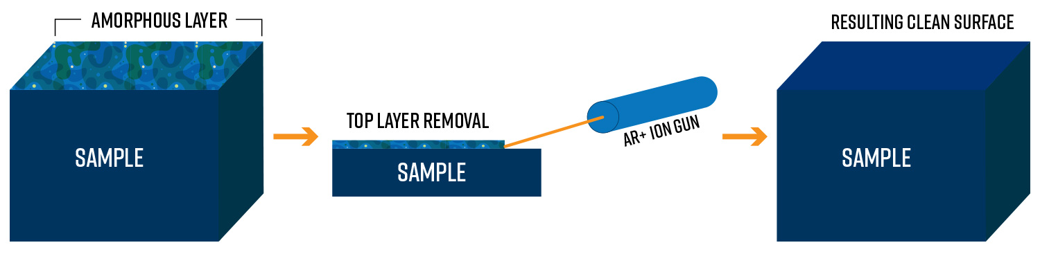
Ion milling devices, often referred to as ‘cross-section polishers,’ are equipped with a range of capabilities that amplify their utility in laboratory settings. For instance, systems like the SEMPrep2 ion mill provide an impressive toolkit that includes both high and low energy ion guns capable of generating ion beams ranging from 100 eV to 16 keV. Additionally, these systems feature adjustable tilting mechanisms for slope cuts, as well as in-plane oscillation and rotation capabilities, ensuring the evenness and uniformity of the sample surface. The operational area of these instruments can span 1-2 mm in width and 100-300 µm in depth, granting researchers unparalleled flexibility and control over their sample preparation processes.
While ion milling is useful for preparing entire cross-sections or precise slope cuts, the efficiency of material removal depends on the thickness of the sample; it follows that the more material there is, the longer the milling process will take. However, the real value of ion milling is realized when it is integrated as the final step in a multistage preparation process.
Cross-Sectional Sample Preparation Workflow
A typical workflow might begin with an initial cut using a diamond saw to rapidly expose the inner layers of the material. This is followed by mechanical polishing to smooth the surface, removing some damage from the cutting process and creating a more planar surface. Using ion milling as the finishing touch achieves a pristine surface ready for detailed analysis of a sample material’s subsurface features using SEM. The initial rough cuts and mechanical polishing quickly reduce the sample to near-final dimensions, while the ion milling process refines the surface to an exceptional degree of smoothness and uniformity. This general workflow is suitable for a variety of sample types including semiconductor packages, batteries, and geology specimens.

Semiconductor Packaging
Ion milling’s utility extends across various industries, particularly in failure analysis. SEM and EDS techniques applied to good cross-sections help identify internal failures or defects in manufactured devices [1]. This level of analysis is essential for examining features related to failures such as crack propagation, fracture modes, corrosion, solder joints, physical damage, delamination, and coating failures.
To demonstrate the effectiveness of ion milling for analyzing packaged semiconductor chips, a sample was prepared by a multi-step preparation process involving diamond sawing, mechanical polishing, and finalization with ion milling using the SEMPrep-2 Ion Mill. The samples were imaged after each step using a Phenom Desktop SEM.
Figure 2a, shows the resultant surface after it was sectioned using a diamond saw. The surface was dominated by amorphous material that obscured the sample’s features. While some compositional differences were indicated by the contrast from backscattered electrons, these contrasts could not compensate for the distortion caused by rough, uneven, and deformed features. The sample then underwent mechanical polishing, using varying grits (600, 800, 1000, and 1200 at 100 rpm) followed by a finer polish with diamond paste at 200 rpm. Subsequent SEM imaging revealed more defined layers and boundaries and the internal structure gradually became more discernible as shown in Figure 2b. However, the presence of amorphous material still covered much of the cross-section, indicating the need for further refinement. The surface was then ion milled which effectively removed the residual amorphous material, unveiling well-defined, clear layers of the semiconductor material. The structures were now completely free from artifacts and brought a significant amount of clarity to the sample allowing for highly detailed cross-sectional analysis (Figure 2c).
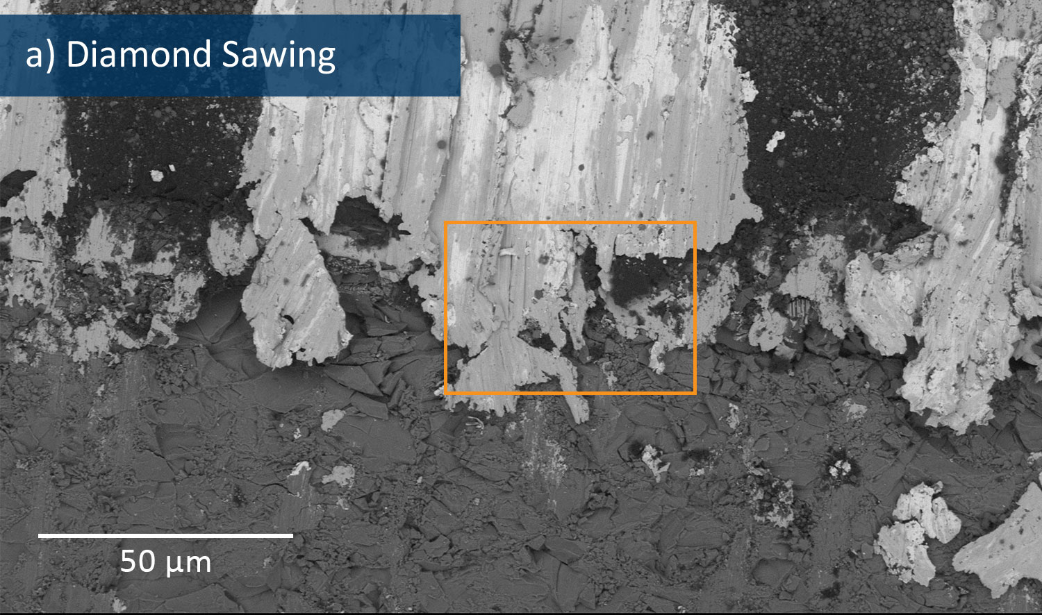
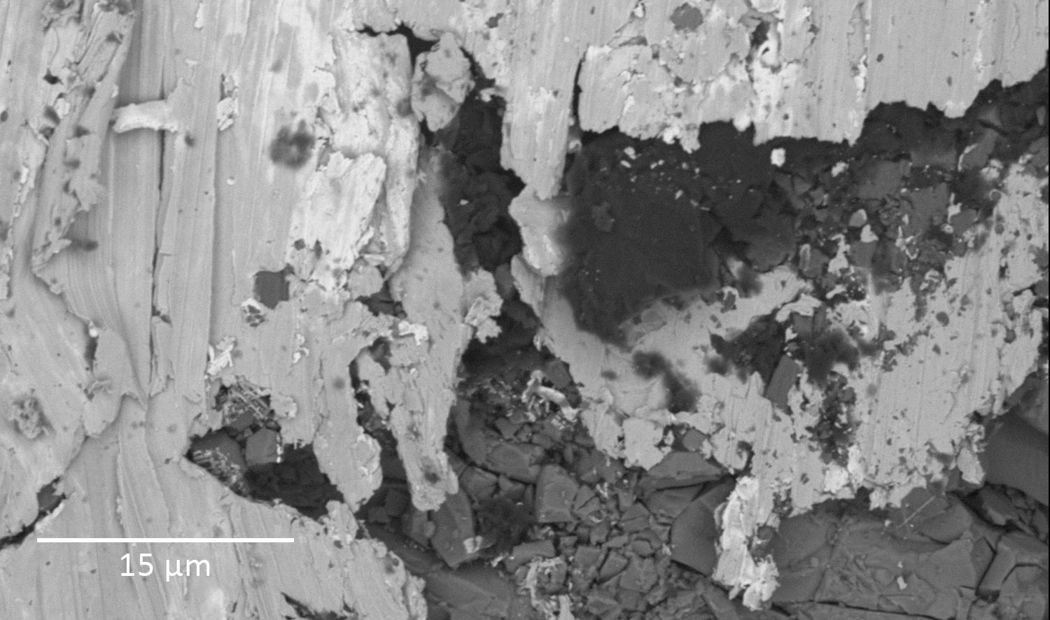
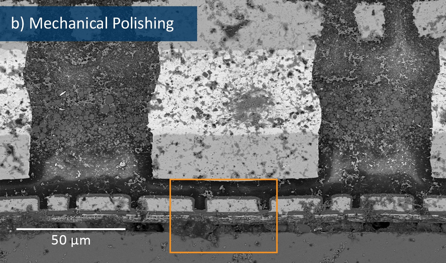
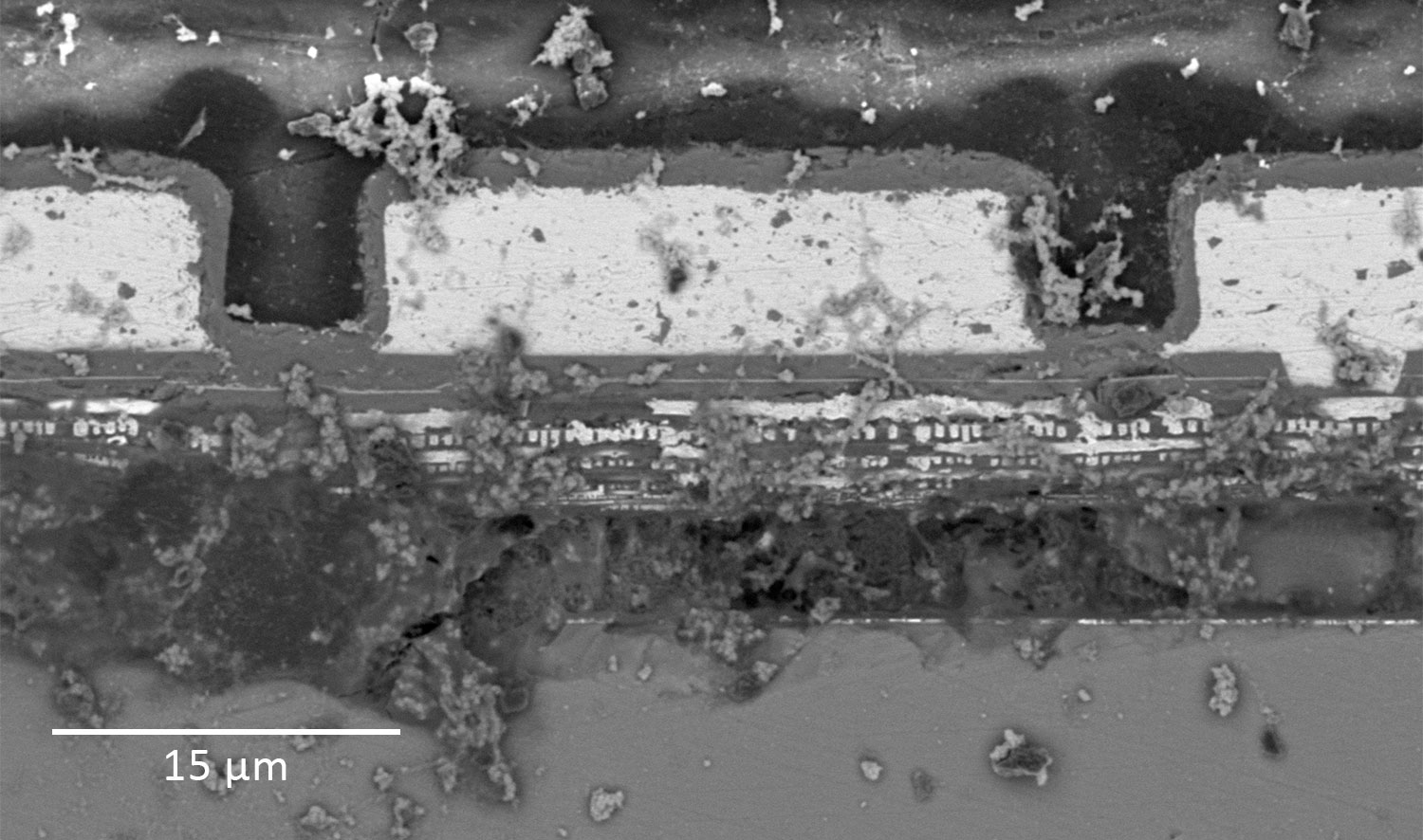
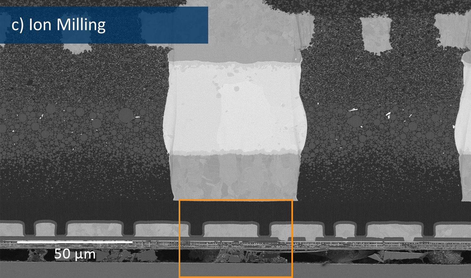
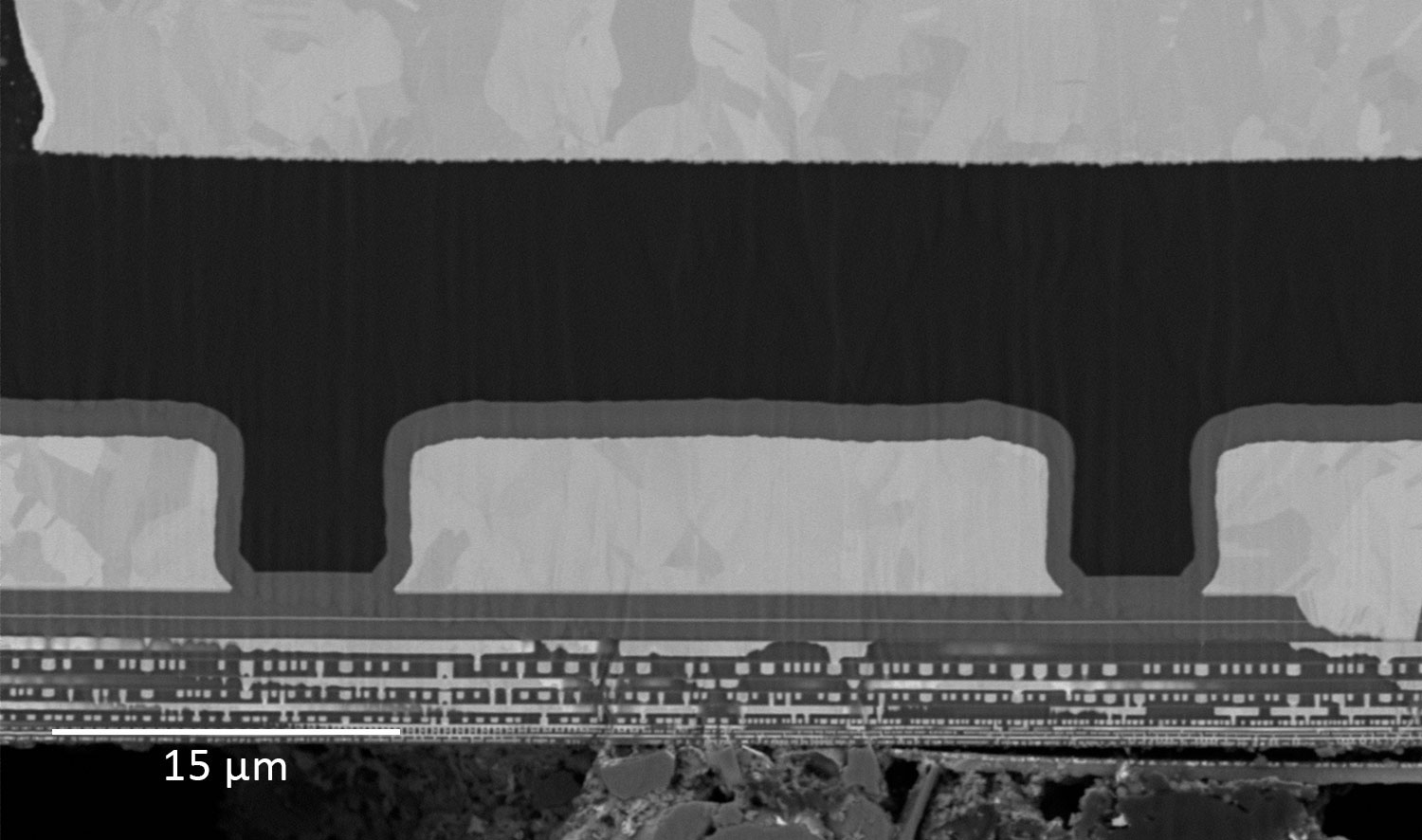
Figure 2. SEM micrographs collected after (a) diamond sawing, (b) mechanically polishing, and (c) ion milling a semiconductor substrate.
The importance of clean cross-section and amorphous material on elemental analysis is highlighted in Figure 3. In this figure, EDS elemental abundance maps are false-colored to enhance the identification of elements. The maps clearly show how the smeared or uneven material layers can hinder accurate elemental analysis by either emitting X-rays from the distorted material or absorbing them, thus obscuring the true elemental composition of the substrate. The EDS map of the substrate after sectioning using a diamond saw, as shown in Figure 3a. This method resulted in the poorest quality of the EDS maps, as evidenced by a directional smear across the Ni/Sn/Cu interconnects and the Cu metallization layers. This distortion severely compromised the ability to accurately measure layer thicknesses or to assess potential contamination resulting from process defects. Mechanical polishing of the surface cleaned up the surface to a moderate degree; however, significant contamination was observed within the Sn interconnects, which likely resulted from residues left by the mechanical polishing process (Figure 3b). While the overall surface appeared cleaner than after sawing, these remnants of contamination still posed a challenge for precise elemental analysis.
Ion Milling proved highly effective in removing the contaminations left by previous processes, producing a surface conducive to reliable EDS analysis (Figure 3c). The cleaned surface revealed a small amount of Ti scattered throughout the tin and copper sections, indicating the presence of elements that were previously obscured by the smears and contaminations.
Ion milling, therefore, not only enhances the visual clarity of SEM images but also significantly improves the accuracy of EDS maps. This step is essential for obtaining true material characteristics and ensuring that EDS data are reflective of the actual sample composition, free from the artifacts and distortions introduced during earlier preparation stages.
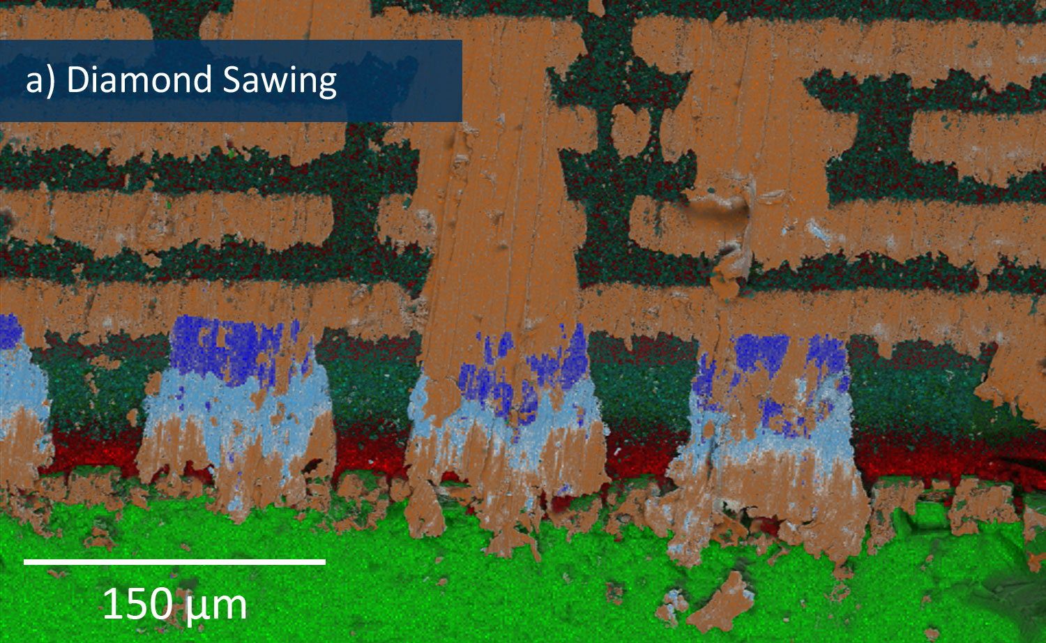
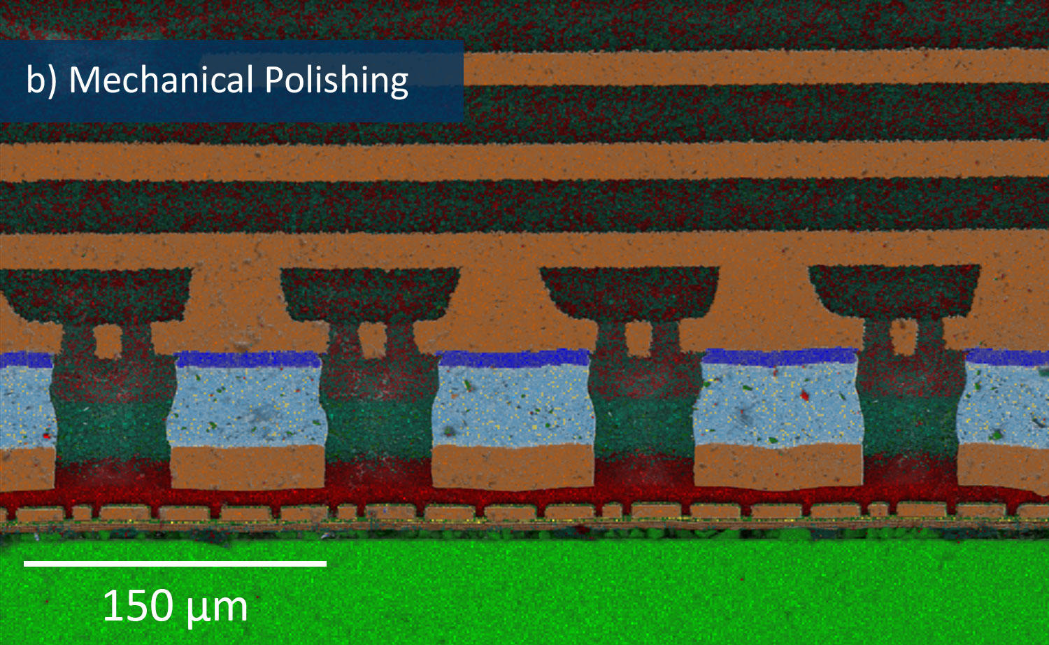
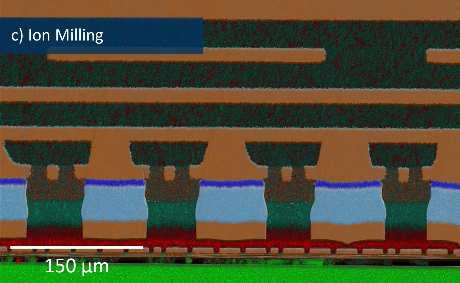
Figure 3. EDS maps obtained after (a) diamond sawing, (b) mechanically polishing, and (c) ion milling a semiconductor substrate.
Batteries and Energy Storage Materials
The performance of batteries is fundamentally influenced by the size, morphology, and composition of electrode active materials. Understanding these aspects is crucial, and cross-sectional SEM analysis provides precision to characterize these critical features of a battery’s microstructure [3]. However, the challenge arises when dealing with batteries that incorporate multiple interfaces composed of thin films, powders, and organic separators. Achieving a clean, planar surface that is free of damage during cross-sectioning is essential to accurately revealing details such as grain structures, particle size distributions, and layer thicknesses.
To illustrate the effectiveness of ion milling in battery research, a Li-ion battery cathode tape was cross-sectioned using a sharp scissors, a method that, while quick, typically results in a rough, uneven surface that does not adequately expose the internal structure necessary for high-resolution analysis. Figure 4a shows a SEM image of as-cut surface where the internal structures of the Nickel Cobalt Manganese (NCM) particles remain obscured, making it difficult to conduct a thorough analysis. Subsequent ion milling drastically improved the quality of the surface (Figure 4b). The milling process revealed not only the individual NCM particles but also the differentiation between the binder material and the particles themselves. This clarity is essential for accurately assessing the microstructural characteristics of the cathode material.
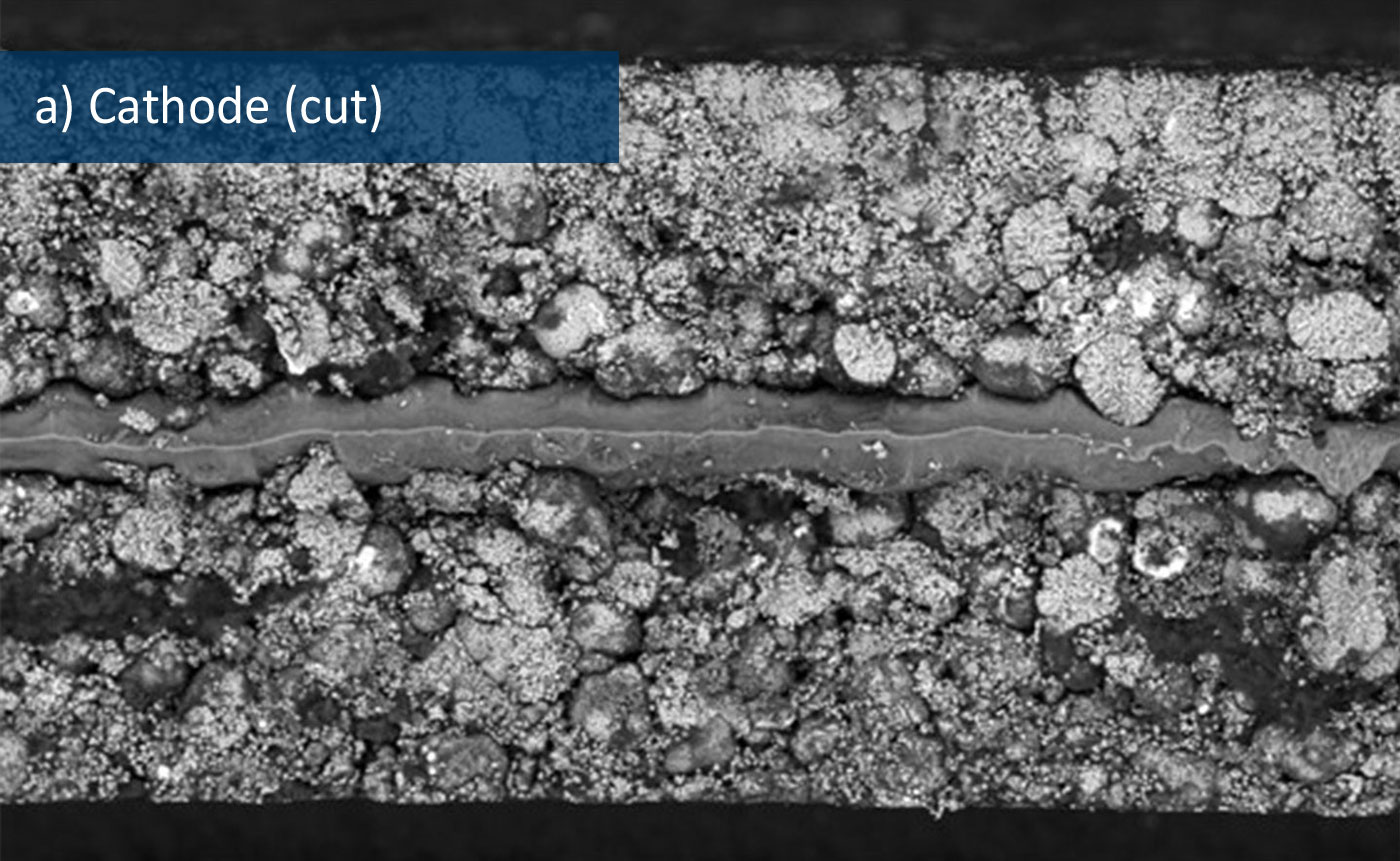
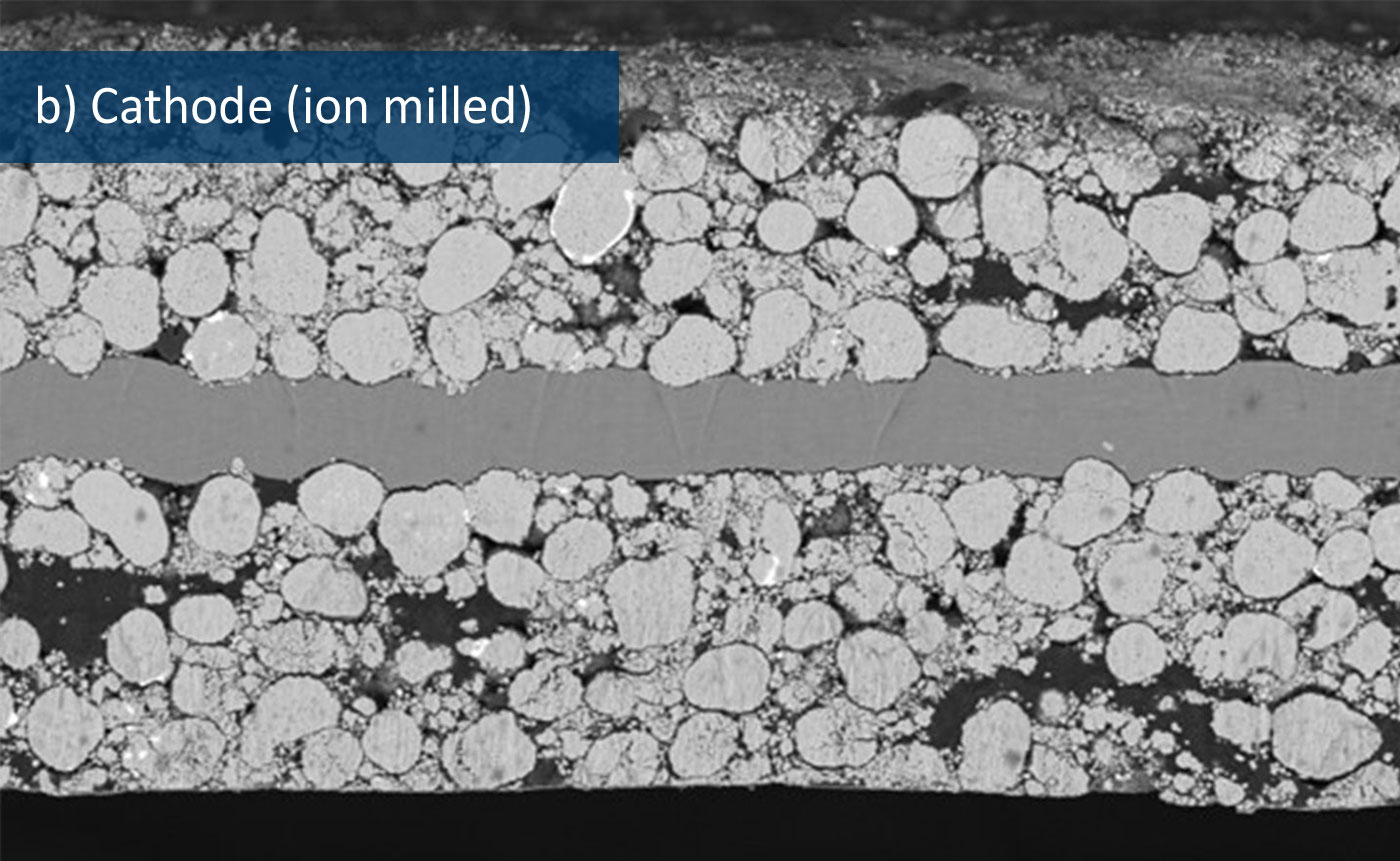
Figure 4. Backscattered Electron SEM images of a Li-ion battery cathode tape (a) cut and (b) ion milled.
Conclusion
The effective preparation of material cross-sections plays a pivotal role in microanalysis, enabling the in-depth study and understanding of a material’s internal structures and characteristics. Ion milling is a valuable technique for achieving artifact-free surfaces that are ideal for detailed SEM and EDS analyses. This method ensures that subsurface features, such as layers, grains, interconnections, and other microstructural elements, are accurately exposed and preserved for evaluation.
The consistent application of ion milling in cross-sectional sample preparation not only enhances the reliability of the analytical results but also mitigates the risks of drawing incorrect conclusions from damaged or obscured surfaces. Integrating ion milling as a final step following initial cutting and mechanical polishing lets researchers maintain the integrity of the material’s microstructure, thereby gaining a true representation of its characteristics.
References
[1] Grosshardt, O., Nagy, B.Á. & Laetsch, A. Applying microscopic analytic techniques for failure analysis in electronic assemblies. Appl. Microsc. 49, 7 (2019). https://doi.org/10.1186/s42649-019-0009-1
[2] Nowakowski P, Ray M, Fischione P. Millimeter-scale, Large Uniform Area Semiconductor Device Delayering for Physical Failure Analyses and Quality Control. Microscopy and Microanalysis. 2022;28(S1):3184-3187. doi:10.1017/S1431927622011825
[3] Jinchao Liu, Yinlong Wu, Shiheng Yin, Xianfeng Yang, and Shuqin Song. Cathode Evolution Track for Evaluating Commercial Lithium-Ion Battery Attenuation through Ar Ion Beam Cutting Energy & Fuels 2023 37 (13), 9662-9671 DOI: 10.1021/acs.energyfuels.3c01099