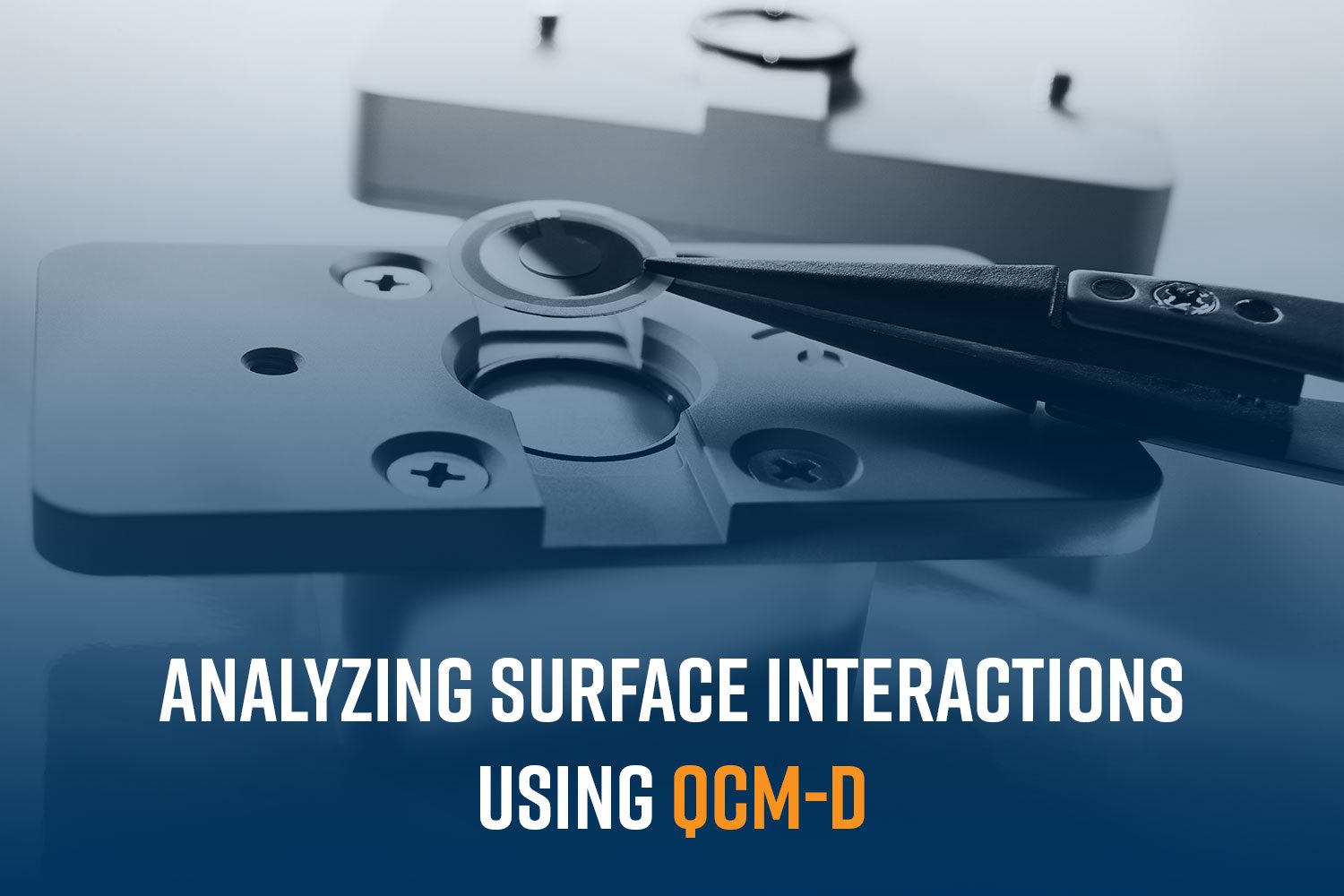
Quartz Crystal Microbalance with Dissipation Monitoring (QCM-D) is a versatile analytical technique that can provide real-time, quantitative data on mass changes and viscoelastic properties of…
Posted: December 18, 2024 | Technology: QCM-D

Optical tensiometers, also referred to as goniometers, drop shape analyzers, or contact angle meters, are indispensable instruments used in scientific and industrial applications requiring precise…
Posted: December 11, 2024 | Technology: Tensiometry

In the world of material fabrication, various techniques have emerged to create complex and functional materials for a wide range of applications, from medical devices…
Posted: December 4, 2024 | Technology: Electrospinning & Electrospraying

Optical tensiometers, also referred to as goniometers, contact angle meters, or drop shape analyzers, are essential tools in materials science, enabling precise measurements of surface…
Posted: November 20, 2024 | Technology: Tensiometry
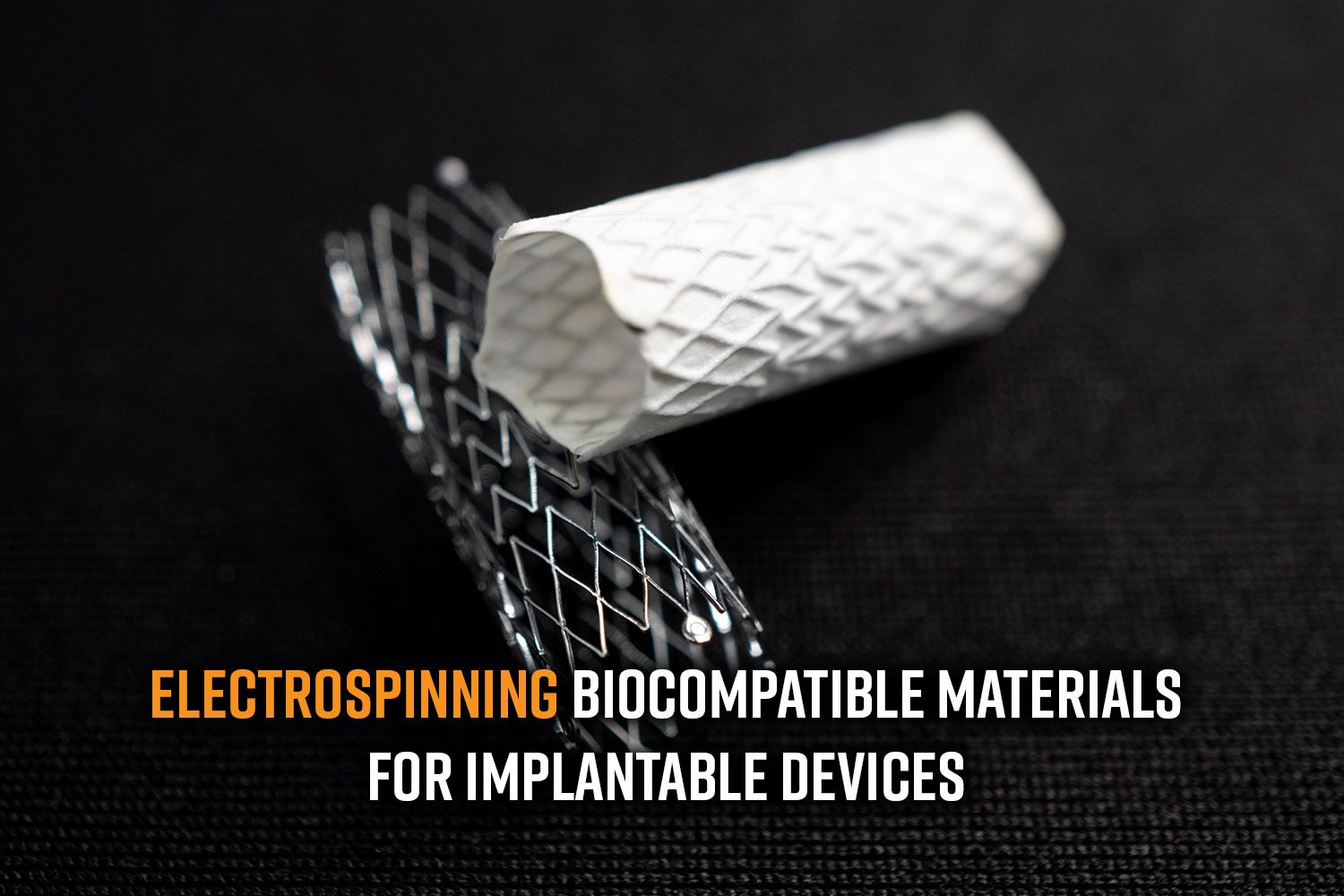
The need for implantable devices and biocompatible materials is driven by the demand for advanced medical solutions that can repair, replace, or support damaged tissues…
Posted: November 13, 2024 | Technology: Electrospinning & Electrospraying

In the age of climate change and resource depletion, the circular economy is increasingly gaining attention. It promotes the reuse, recycling, and repurposing of materials…
Posted: November 6, 2024 | Technology: Scanning Electron Microscopy

Energy dispersive spectroscopy (EDS) is a microanalysis technique that provides localized elemental composition data, typically used in conjunction with scanning electron microscopy (SEM). While SEM-EDS…
Posted: October 30, 2024 | Technology: Scanning Electron Microscopy

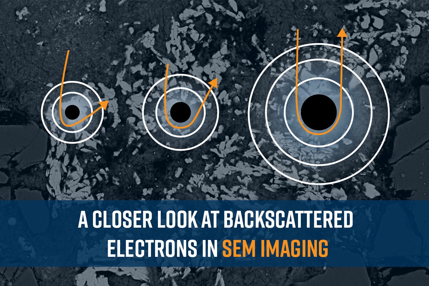
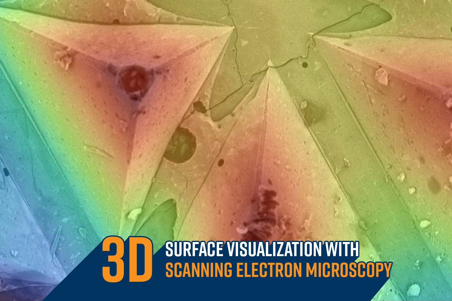
The ability to precisely analyze a material’s structure and composition at the microscopic scale is essential for advancing research and innovation. Scanning electron microscopy (SEM)…
Posted: October 23, 2024 | Technology: Scanning Electron Microscopy
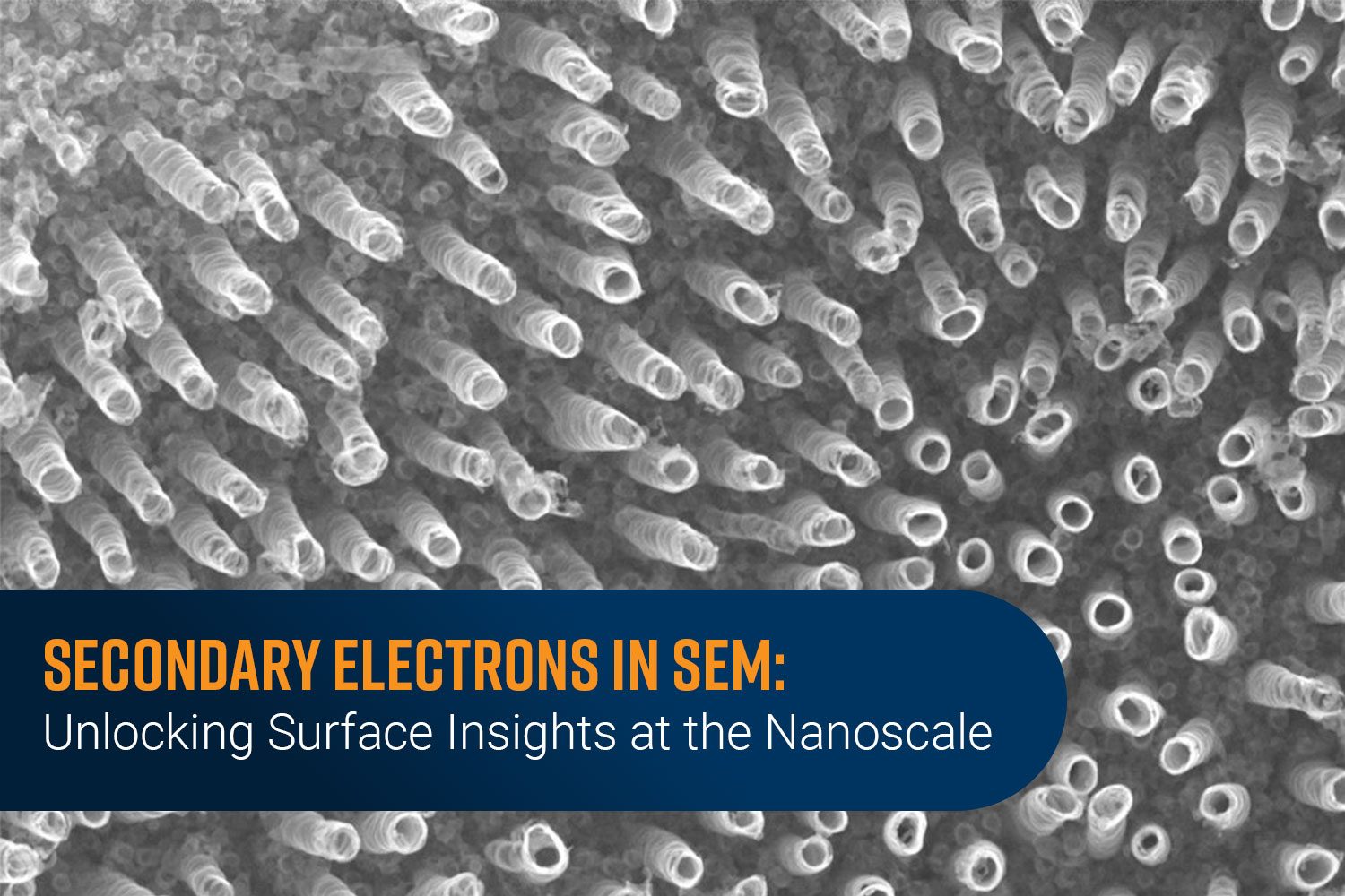
In scanning electron microscopy (SEM), secondary electrons (SE) play a pivotal role in revealing the surface details of materials at the nanoscale. Understanding what secondary…
Posted: October 16, 2024 | Technology: Scanning Electron Microscopy
Materials scientists leverage a range of advanced analytical techniques to extract detailed information regarding a sample’s structure, properties, and defects. Scanning electron microscopy (SEM) is…
Posted: October 9, 2024 | Technology: Scanning Electron Microscopy
Scanning electron microscopy (SEM) has long been a cornerstone in material science, biology, and engineering for its ability to provide high-resolution images of a sample’s…
Posted: October 2, 2024 | Technology:

Quartz Crystal Microbalance with Dissipation Monitoring (QCM-D) is a powerful sensing technique that allows researchers to investigate real time changes in nanoscale mass and viscoelastic…
Posted: September 25, 2024 | Technology: QCM-D