
Integrating the ability to perform high-resolution imaging and compositional analysis of materials into any laboratory becomes simplified with a desktop scanning electron microscope (SEM). In…
Posted: April 10, 2024 | Technology: Scanning Electron Microscopy

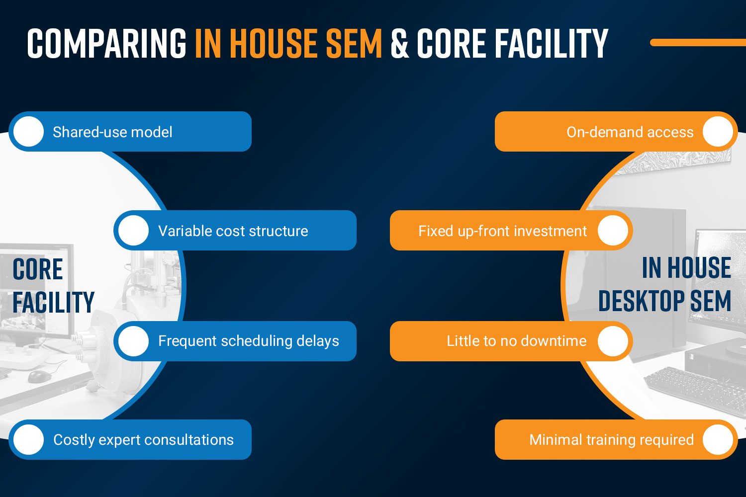
When acquiring a new scanning electron microscope (SEM), it can be challenging to identify a solution that not only delivers exceptional performance but also remains…
Posted: April 5, 2024 | Technology: Scanning Electron Microscopy
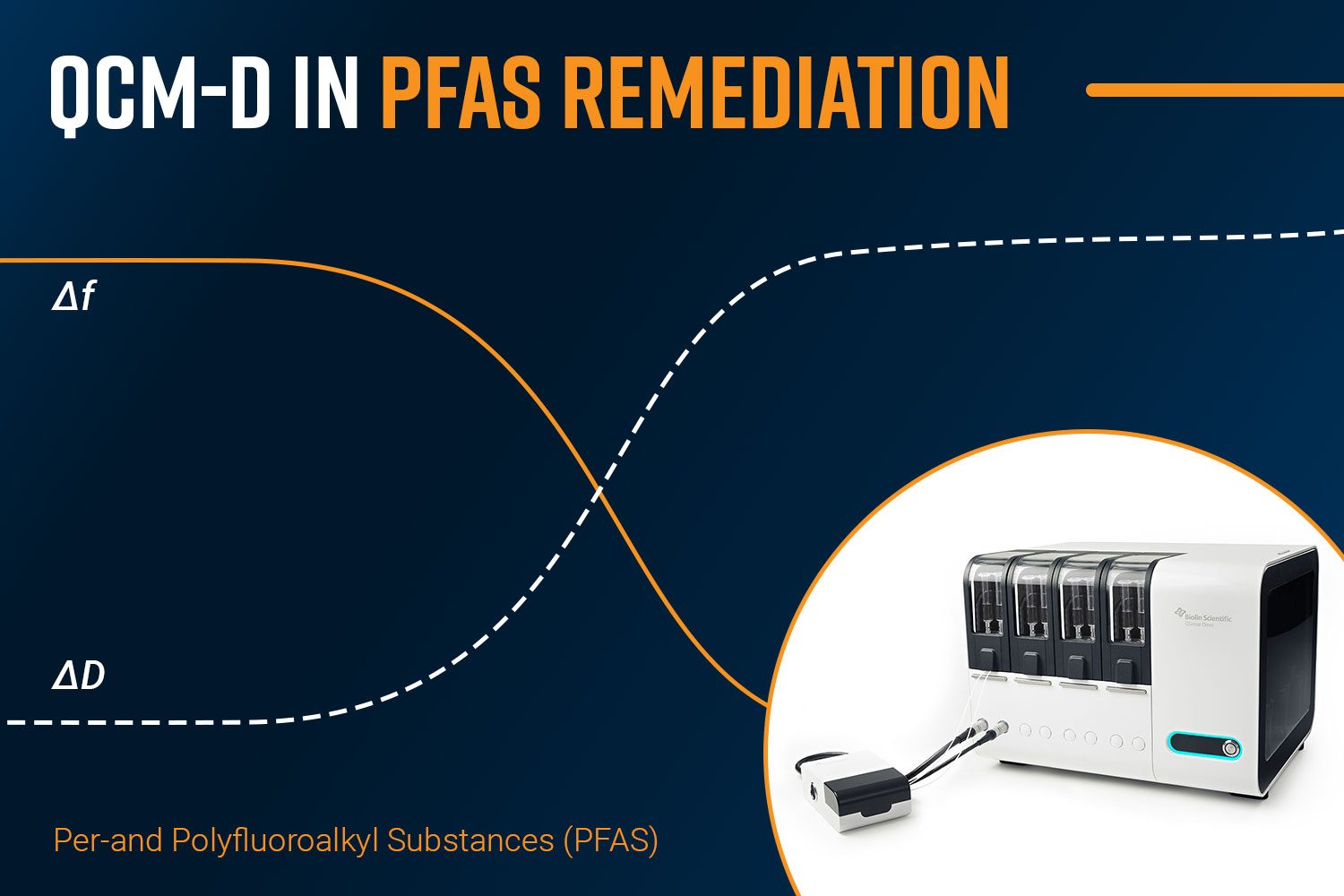
Per- and PolyFluoroAlkyl Substances (PFAS) have been widely used in a range of applications. The concern with PFAS arises from their persistence in the environment…
Posted: April 3, 2024 | Technology: QCM-D

Precision manufacturing is a process that emphasizes exact specifications and extremely tight tolerances within fabricated components. Within this domain, the term technical cleanliness (TC) refers…
Posted: March 27, 2024 | Technology: Scanning Electron Microscopy
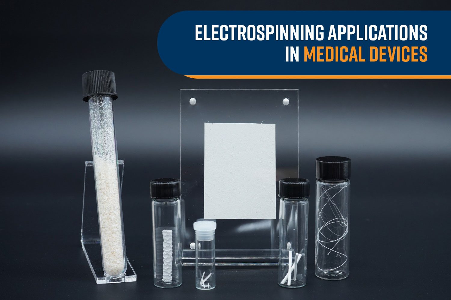
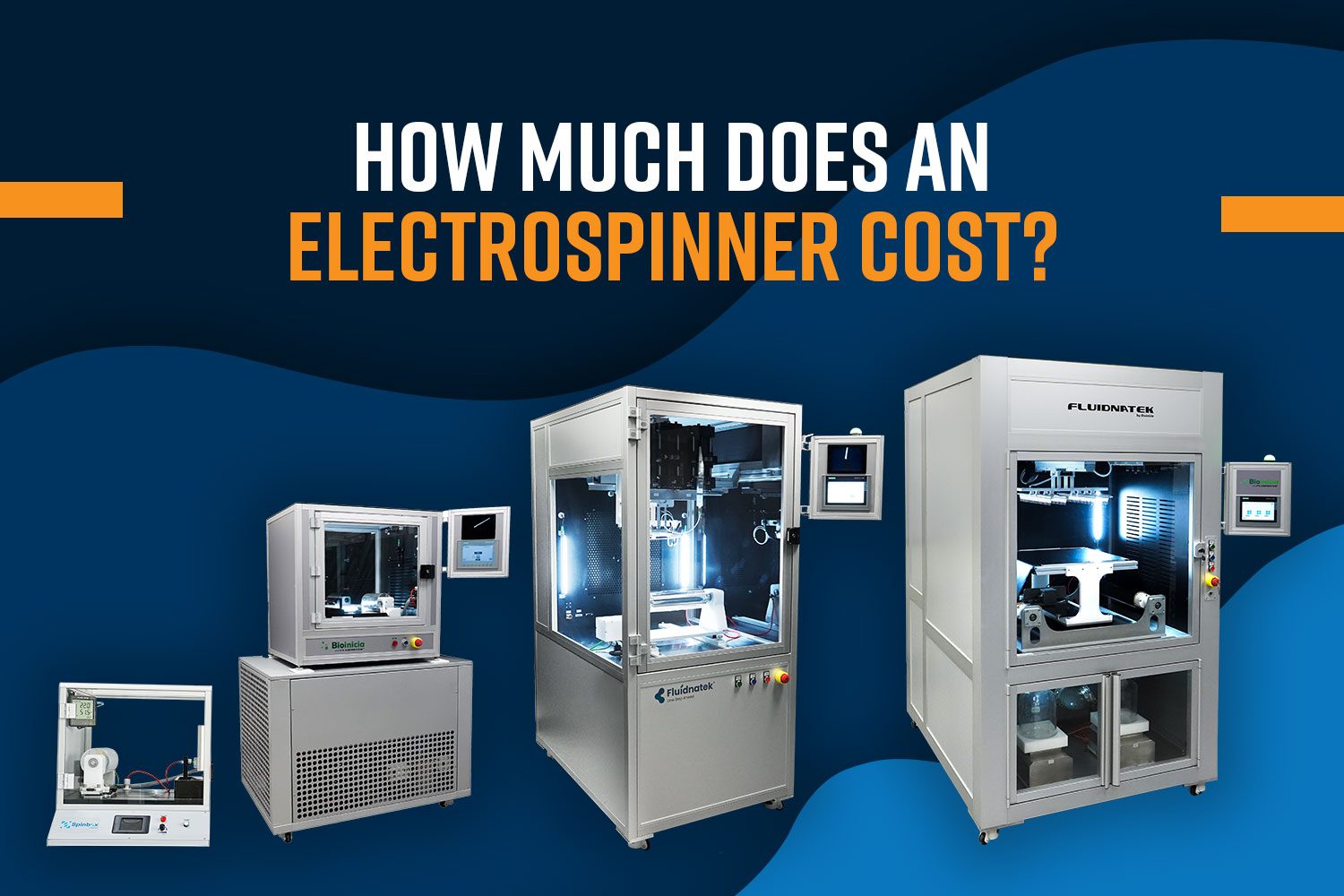
Electrospinning is an emerging technology in the medical device industry, offering precise control over material properties and structure at the nanoscale. Its ability to produce…
Posted: March 20, 2024 | Technology: Electrospinning & Electrospraying
Scanning electron microscopy (SEM) is an essential tool that allows scientists to directly visualize the surface structure and composition of a variety of materials on…
Posted: March 13, 2024 | Technology: Scanning Electron Microscopy

Microscopes have revolutionized our ability to observe and analyze the microscopic world with unprecedented detail. By enlarging our view of objects, or magnifying them, microscopes…
Posted: February 28, 2024 | Technology: Scanning Electron Microscopy

In the evolving landscape of pharmaceutical research and development, the goal to understand the micro and nanoscale properties of therapeutics is vital. Central to this…
Posted: February 14, 2024 | Technology: Scanning Electron Microscopy

Contact angle is defined as the angle formed by a liquid at the three-phase boundary where the liquid, solid, and gas intersect. It gives a…
Posted: February 7, 2024 | Technology: Tensiometry
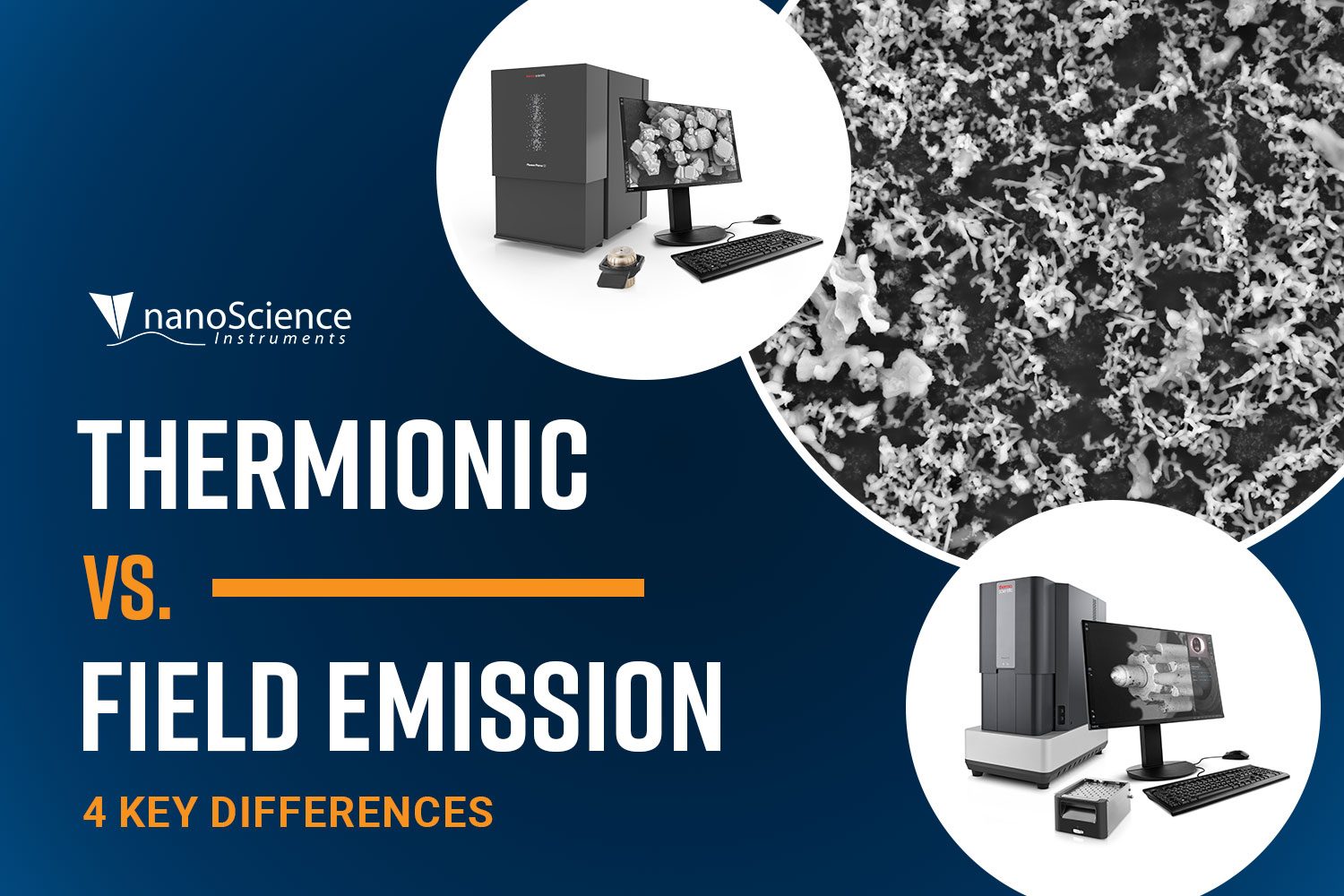
The electron source is one of the most critical components of a scanning electron microscope (SEM) because it determines the quality, brightness, and size of…
Posted: January 31, 2024 | Technology: Scanning Electron Microscopy
Electrospinning and electrospraying technologies continue to gain prominence due to their versatility in nanofiber and nanoparticle development. Researchers, scientists, entrepreneurs, and industry professionals face the…
Posted: January 17, 2024 | Technology: Electrospinning & Electrospraying
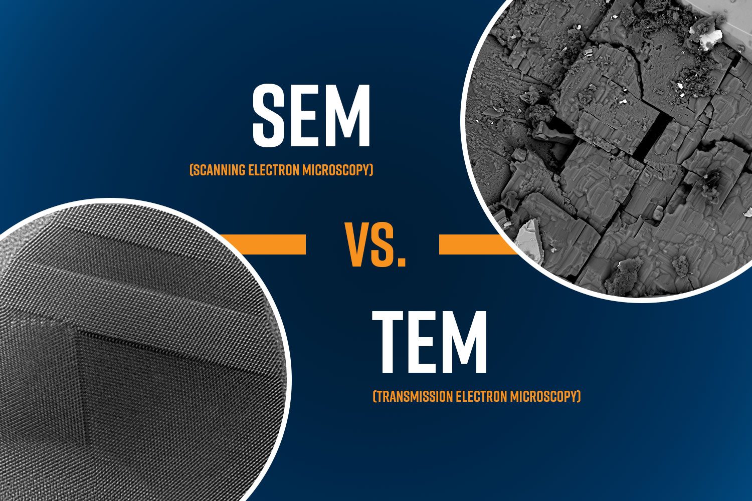
Electron microscopy is best known as a high-powered microscopy technique that utilizes a beam of electrons as a source of illumination. In an electron microscope,…
Posted: January 10, 2024 | Technology: Scanning Electron Microscopy