In scanning electron microscopy (SEM), secondary electrons (SE) play a pivotal role in revealing the surface details of materials at the nanoscale. Understanding what secondary electrons are, how they are generated, and what kind of information they provide is essential for anyone interested in material characterization, nanotechnology, or surface science. This blog will take a deep dive into secondary electrons and what we can learn from them in SEM imaging.

What are Secondary Electrons?
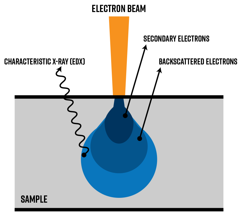
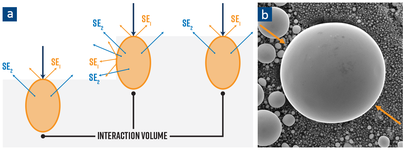
SEs are weakly bound (outer shell) electrons that are ejected from the sample’s constituent atoms as a result of inelastic scattering with the incident electron beam in the SEM (Figure 1). These electrons have kinetic energies of less than 50 eV and can easily be re-scattered within the material. Therefore, the detected SE signal is localized to a shallow depth within the sample surface of around less than 10 nanometers.

Because most of the detected SEs are generated from very shallow depths (about less than 10 nanometers), they provide information that is highly sensitive to surface features. The smaller interaction volume contributing to the SE signal, compared to that of backscattered electrons (BSEs), means that SE images also demonstrate superior spatial resolution (Figure 2). SEs are collected by an SE detector, often called an Everhart-Thornley detector (ETD), which converts the electron signal into an image.
The number of secondary electrons produced depends on several factors, including:
- Beam energy: Lower beam energies tend to produce more secondary electrons as they are more likely to interact with the surface layer.
- Angle of incidence: A shallow angle between the primary beam and the surface will produce more SEs because more of the interaction volume intersects the surface region. The same effect can be achieved by tilting the sample toward the SE detector.
- Material type: Insulating materials tend to generate more secondary electrons compared to conductive materials due to their low conductivity, which causes the primary electrons to become localized at the surface. In some cases, this excess signal can lead to unwanted charging effects which can obscure the image by producing a washed-out image.
What are SE1, SE2, and SE3 Signals?
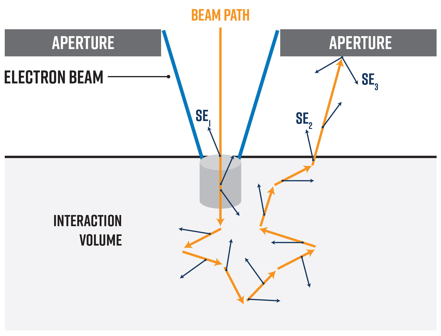
To optimize SE imaging, it is important to understand all the signals that can contribute to a SE image acquired in the SEM. There are three types of SEs that can be detected by a SE detector: SE1, SE2, and SE3 (Figure 3).1 The SE1 signal are true SEs that originate from the region where the electron beam is incident on the sample, causing the emission of inelastically scattered electrons. This signal conveys the highest resolution information. A SE2 is a BSE that is inelastically scattered in the sample, emerges from the surface and is then detected by the SE detector. BSEs are much higher in energy and are generated from a much larger, and deeper interaction volume. The SE2 signal can degrade the overall resolution by adding sub-surface information. SE3s are generated when a BSE strikes anything other than the sample, such as the pole piece or specimen chamber. They add overall noise to the image. In general, lower accelerating voltages can improve the ratio of SE1 to SE2 because the interaction volume is decreased, leading to less spread of the BSE signal.
What Can We Learn from Secondary Electrons?
Secondary electrons provide highly detailed surface information. Since SEs are sensitive to topographical changes, the images generated give a clear, high-contrast view of the surface’s texture, ridges, and valleys. The key insights we can gain from secondary electron imaging include:
- Surface Morphology: SE imaging is excellent for visualizing the fine surface structures of a material. Features like cracks, pores, peaks, and valleys are clearly visible in SE images. This is why SE imaging is often used in materials science to study surface defects and fracture patterns.
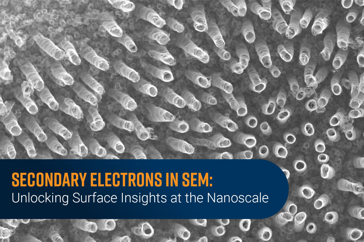
- 3D-like Visualization: Secondary electron imaging gives a quasi-three-dimensional appearance to images due to the way the secondary electrons interact with surface features (Figure 4). This effect can provide a deeper understanding of the sample’s topography, such as relative textural variations between samples if the imaging conditions are held constant. This can be particularly useful in failure analysis, wear testing, and nanostructure characterization.
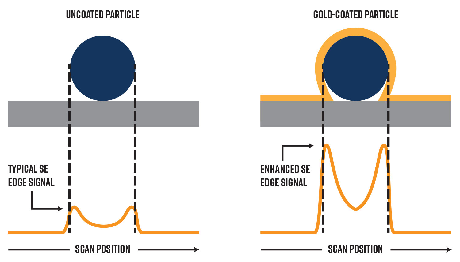
- Edge Effects: One of the distinctive features of SE imaging is the sharp contrast at edges or boundaries. When the primary electron beam interacts with an edge, it tends to produce more SEs, resulting in brighter edges in the SEM image (Figure 5).2 This edge enhancement is useful for identifying boundaries, fractures, or fine features like scratches on the surface.
- Surface Contamination: Because the SE signal is localized to the surface, minute amounts of surface contamination in the form of particles or thin layers can be detected. This makes SE imaging helpful for ensuring that a surface is clean or for identifying unwanted residues during surface preparation or treatment processes.
Sample Coating Effect on SE Signal
A thin metallic coating can be applied to sensitive materials or samples with inherently low SE signal generation to enhance image quality. Metals exhibit a higher SE yield, and by depositing a coating only a few nanometers thick, the sample’s surface morphology remains intact while improving the SE1 signal, which originates directly from the sample surface (Figure 6). The metallic coating does not significantly affect the contributions from SE2 or SE3 signals, preserving the spatial resolution and ensuring the resulting image contains a higher proportion of surface-specific, high-resolution information.
Key Takeaways
SEs are low-energy electrons emitted from the sample surface due to inelastic scattering in the SEM, providing surface-sensitive imaging. In summary, there are a few key points to keep in mind when thinking about SE imaging:
- Surface sensitivity: The surface-localized signal makes SE imaging ideal for topographical analysis and higher resolution imaging
- Factors influencing SE yield: SE production depends on beam energy, angle of incident, and the types of material. Insulators, shallow angles, and lower beam energies generate more SEs, enhancing surface detail.
- SE Signal Types: The SE1 signal, which originates from SEs generated near the surface, provides the highest resolution. SE2 and SE3 signals, from backscattered electrons, add subsurface information but can reduce overall image clarity.
- Improving SE Signals: Thin metallic coatings on samples enhance SE1 signals without affecting SE2 and SE3, preserving high-resolution surface detail.
References
- Y. Liao, “Practical Electron Microscopy Database,” 2006. ↩︎
- P. Zhang, H. Wang, Y. Li, S. Mao and Z. Ding, “Monte Carlo simulation of secondary electron images for real sample structures in scanning electron microscopy,” Scanning, vol. 34, no. 4, pp. 145-150, 2012. https://doi.org/10.1002/sca.20288 ↩︎