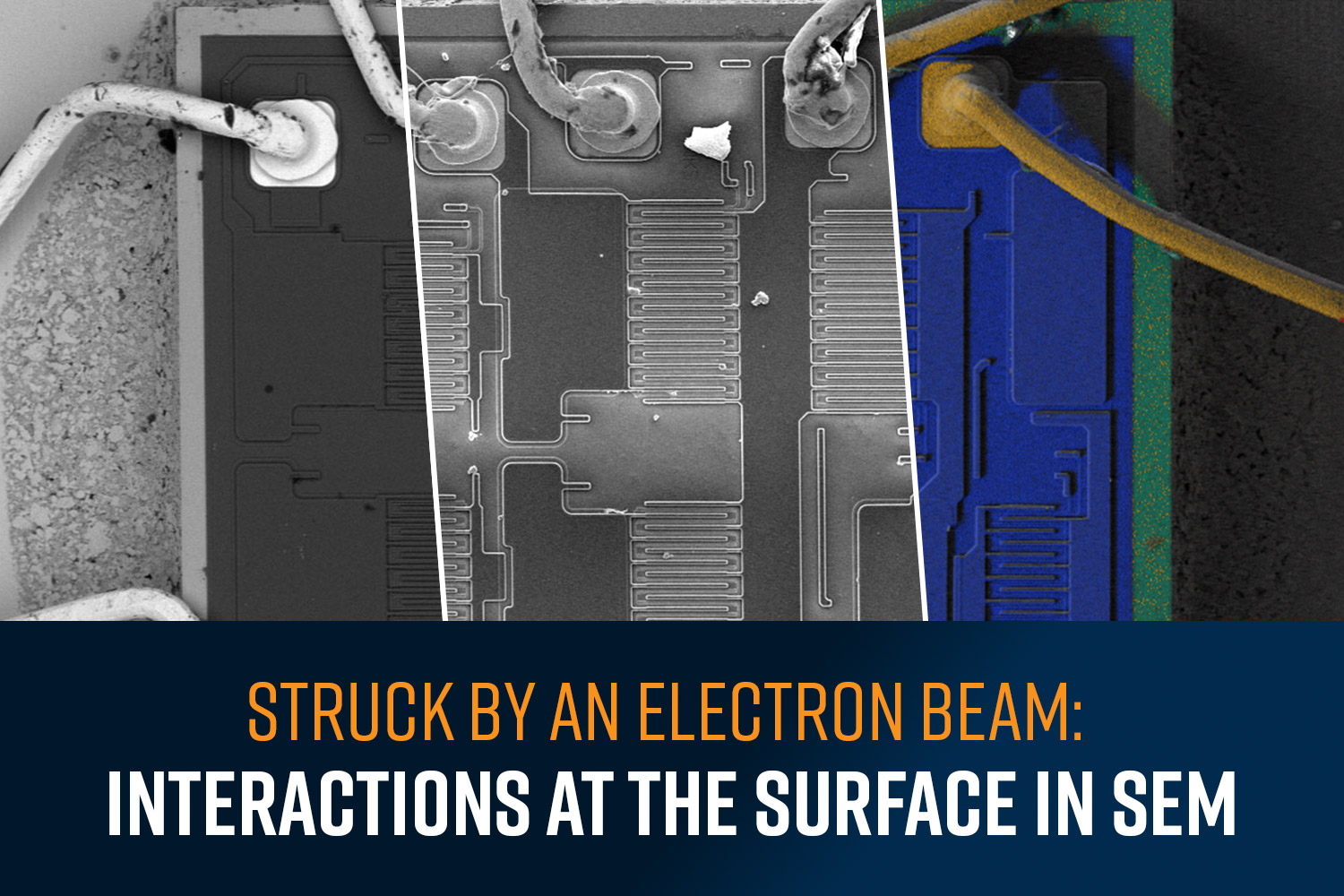
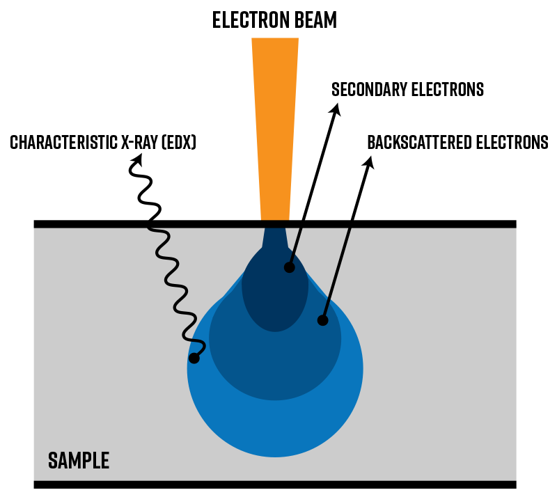
Scanning Electron Microscopy (SEM) is one of the most important tools in the arsenal of modern material science used to characterize micro and nanoscale features. Central to its functionality is the interaction between a finely focused electron beam and the sample. As these electrons meet the surface, they elicit various responses: backscattering, secondary electron emission, X-ray generation, and cathodoluminescence, each carrying unique information about the sample’s composition and structure (Figure 1). These signals can be processed to visualize and better understand the materials.1 This blog examines these interactions, describes how they occur, the types of signals they produce, and the implications of these signals for material analysis.
Figure 1. A schematic depicting the interaction volume of an electron beam striking a sample, along with the resulting electron and X-ray signals.
Electron Beam
A source of electrons, also known as an electron gun, is at the core of an SEM. The electron beam is generated either by thermionic emission or field emission. For instance, the Phenom XL SEM uses a solid-state cerium hexaboride CeB6 crystal (thermionic), whereas the Phenom Pharos SEM employs a tungsten field emission source. The electrons are then accelerated down a column by a potential difference (accelerating voltage) of several tens of kilovolts. The beam is finely focused using electromagnetic lenses, generating a probe that is used to interrogate the sample.
Electron – Surface Interactions
As the electron beam impacts the surface of the sample, several interactions occur that are primarily dependent on the electron energy and the atomic number of the sample material.
Backscattered Electrons (Elastic Scattering)
Backscattered electrons are high energy electrons generated through elastic interactions between the beam and the sample without significant loss of energy. Backscattered electrons originate from a few hundred nanometers of the sample. Backscattered electrons go into the sample, and they pass near a nucleus. The nuclei of the sample produce fields that can sling shot the electron back out of the sample where it can be detected. Elements with large nuclei, which are higher atomic numbers, are more likely to reflect an electron right back out of the sample, whereas a smaller nuclei atom may simply deflect it slightly (Figure 2).
Figure 2. A diagram showing the trajectory of incoming electrons becoming backscattered electrons (BSE) after scattering from nuclei. The larger the nuclei, the more scattering that occurs.
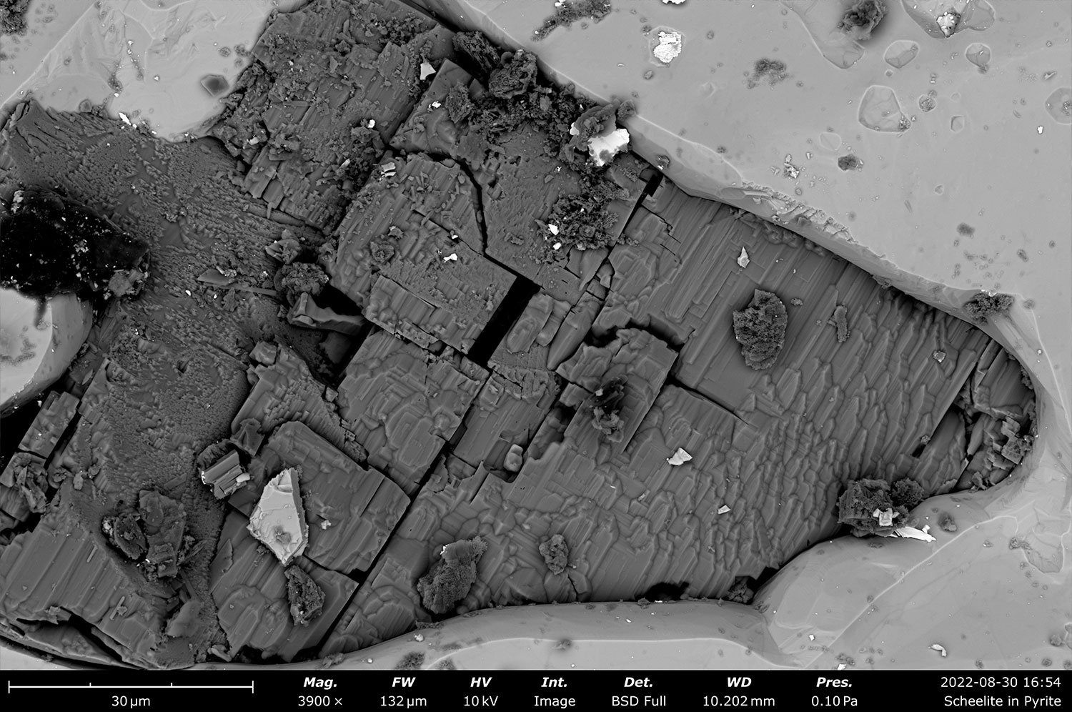
Electrons deflected to a high angle are most likely to leave the sample, which means that heavier elements appear brighter in backscattered electron images. In essence, the number of electrons backscattered during this interaction is proportional to the atomic number of the elements in the sample. Backscattered electron (BSE) imaging conveys information about compositional contrast, as evidenced in Figure 3 with the two compositionally different samples.
Figure 3. Backscattered electron SEM micrographs conveying elemental contrast. The left image is gypsum in pyrite while the right is espresso.
Secondary Electrons (Inelastic Scattering)
Secondary electrons are generated from an electron-electron collision event (inelastic scattering). Secondary electrons are generated when a beam electron displaces a sample electron (Figure 4). The sample electron receives some small remainder of the energy of the incoming beam electron, but much of the beam electron’s energy is lost in the collision. These secondary electrons are thus low in energy, and they can only successfully escape the sample if the interaction happens close to the sample surface.
Figure 4. A diagram of how secondary electrons are generated during electron beam sample interactions.
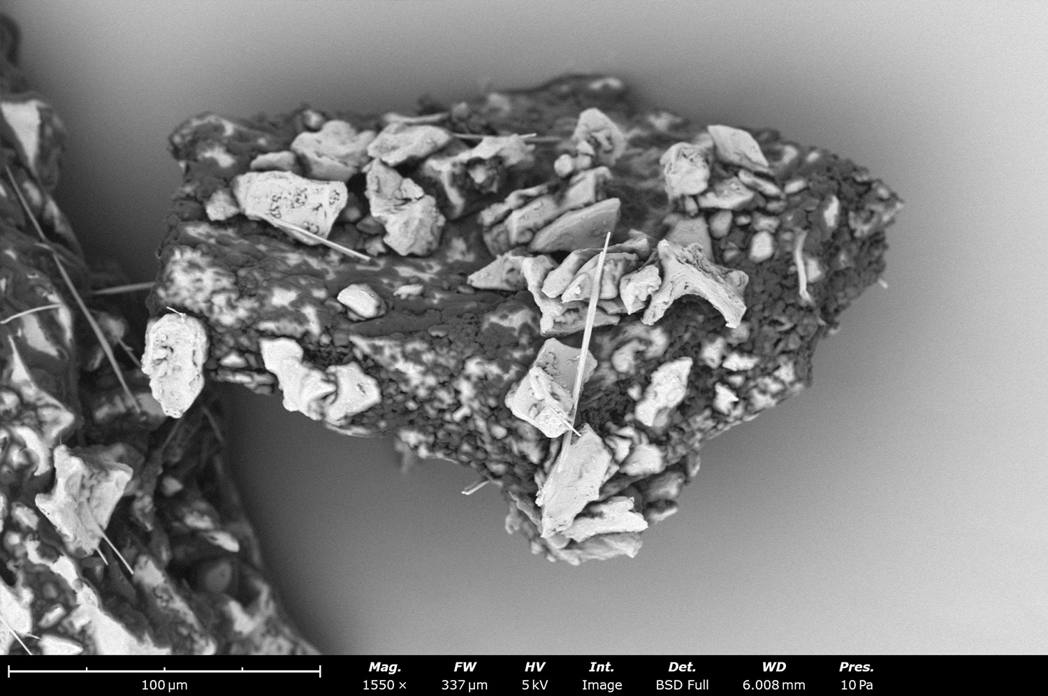
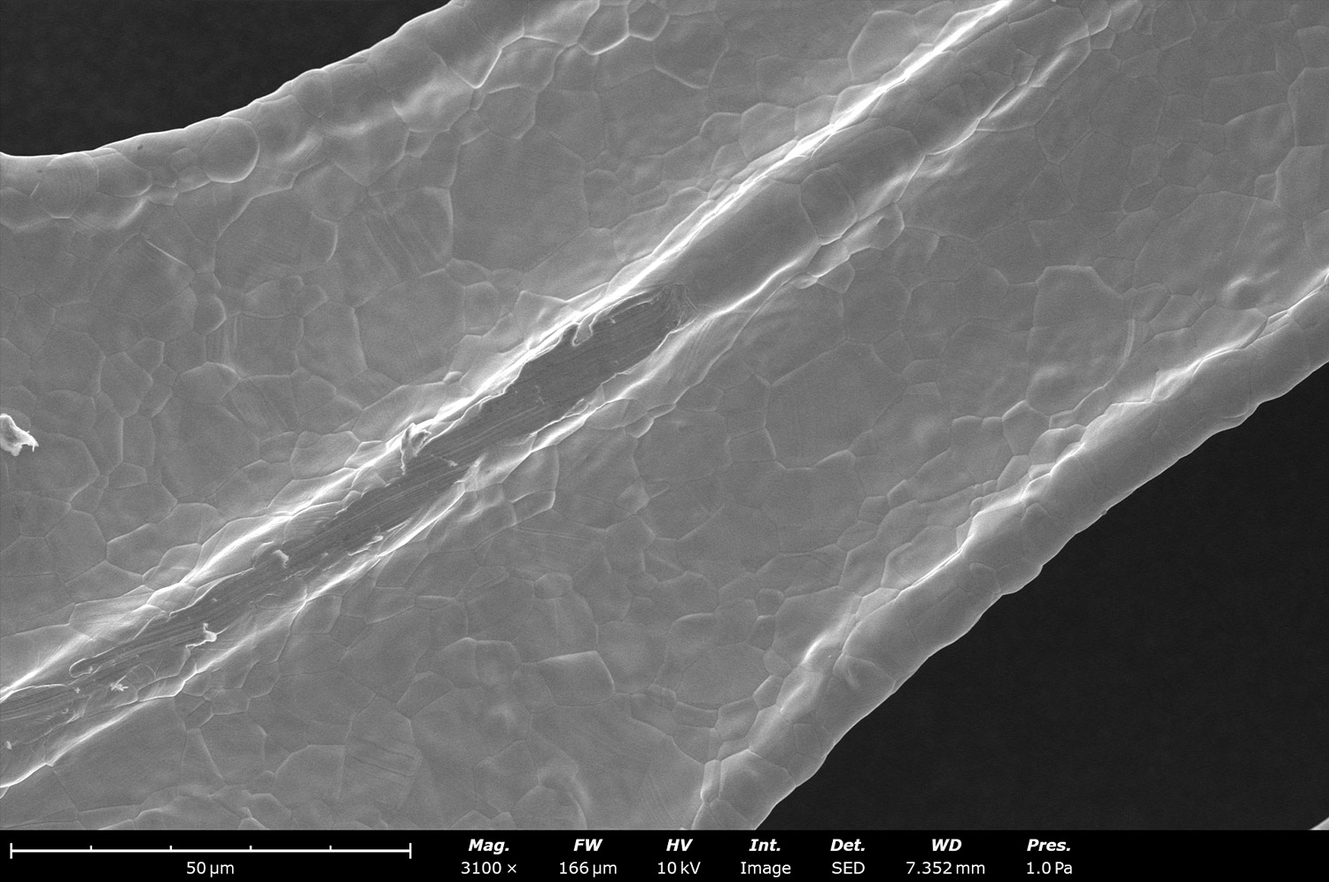
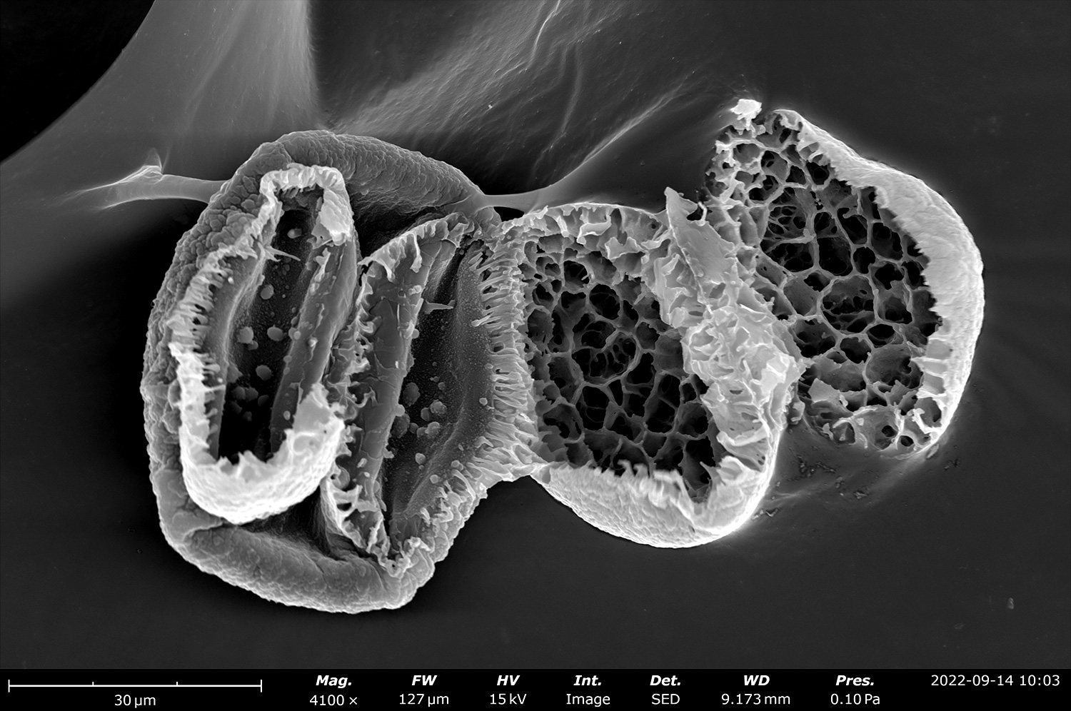
The detectable secondary electrons come from interactions at depths far less than 100 nanometers, which means the electrons carry information from the very surface of the sample. SE imaging is particularly advantageous for revealing a sample’s topography (an example shown in Figure 5) due to the high resolution achievable with these electrons, as they originate very close to the point of impact.
Figure 5. Secondary electron SEM micrographs showcasing the high-resolution strength of SED imaging. The left sample is a ceramic material while the right is a pollen sample.
Characteristic X-Rays (Orbital Shells)
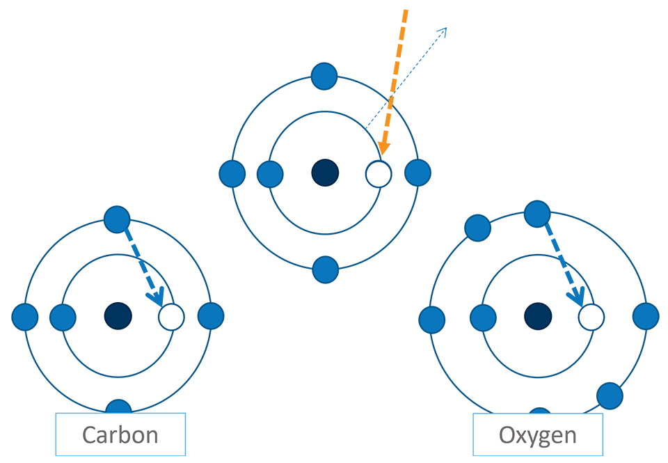
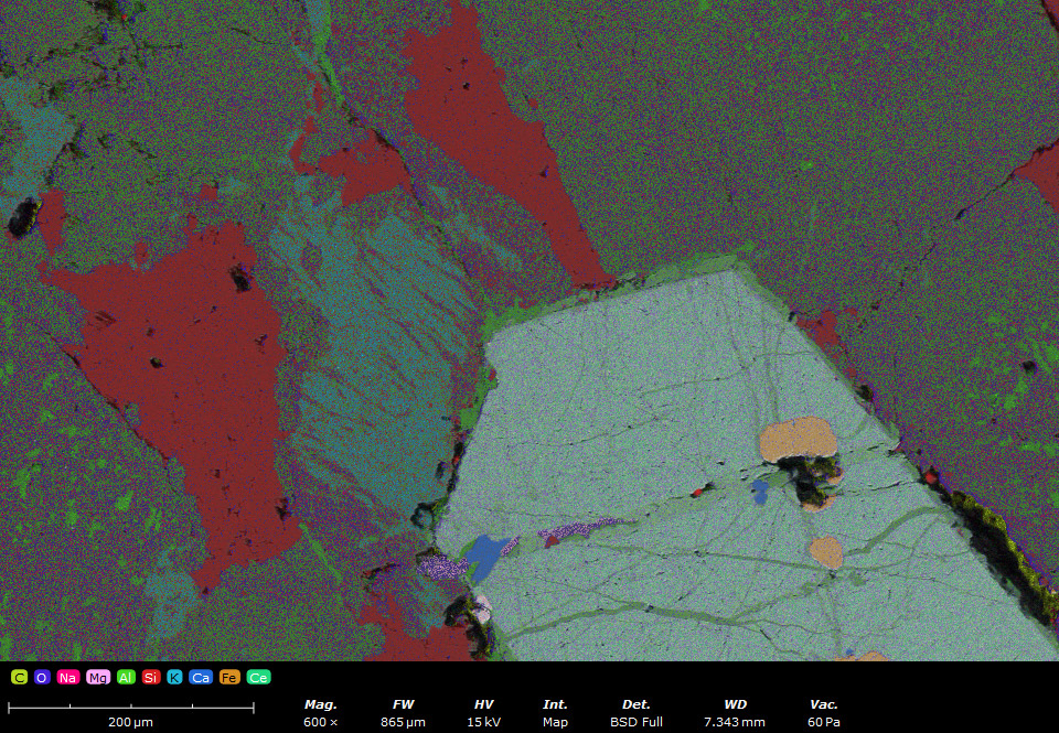
The ionization of atoms can also lead to the emission of characteristic X-rays, which occur when an electron is knocked out of an inner shell. Once it is dislodged, a neighbor electron from a higher shell fall to fill the vacancy, releasing energy in the form of an X-ray (Figure 6). These X-rays are specific to the elements from which they are emitted because their energies can be correlated with the shell transition energies, but some nuanced discrepancies may arise (counting two X-rays, thus doubling the recorded energy); however, there are built in workarounds for some SEM systems. This type of elemental analysis is called Energy Dispersive X-ray Spectroscopy (EDS). An example of elemental characterization using EDS is shown in Figure 7, where 10 elements were identified, measured, and false colored for an abundance map of a common rock.
Figure 6. A diagram showing elemental identification from X-rays with carbon and oxygen as examples. When an electron falls from an outer shell to an inner shell to fill a vacancy caused by the beam, an X-ray is emitted.
Figure 7. An elemental abundance map of a common rock sample, highlighting 10 different elements.
Interaction Influences
Topography and Surface Geometry:
The physical topology of the sample surface influences how electron beam interacts with the sample. Features such as edges, corners, and textured surfaces can significantly affect the trajectory of scattered electrons. These structural variations lead to differences in the emission patterns of both SEs and BSEs, though SEs are used to create detailed topographical maps of the surface. High points and edges tend to emit more SE due to the reduced material surrounding them, enhancing their signal on the SEM image and providing a three-dimensional appearance. Similarly, concave areas may trap electrons, reducing emission and appearing darker.
Surface Roughness:
Surface roughness impacts the way electrons interact with the sample in several ways. Rough surfaces increase the probability of multiple scattering events as electrons are faced with more irregularities. This increased scattering can lead to a higher yield of secondary electrons, which enhances the topographical contrast in the resulting image, but rough surfaces can also complicate image interpretation in some cases. Managing surface roughness through sample preparation techniques such as polishing, or ion milling can help mitigate these issues.
Conclusion
The success of SEM hinges on the interaction of electron beam at the material surface. Understanding these interactions – ranging from the scattering of electrons to the emission of characteristic X-rays – enables researchers to extract detailed information about the sample’s topography, morphology, and elemental composition. Each type of detector inside an SEM plays a big role in converting these interactions into digital signals that form the basis for high resolution imaging and precise analytical measurements.