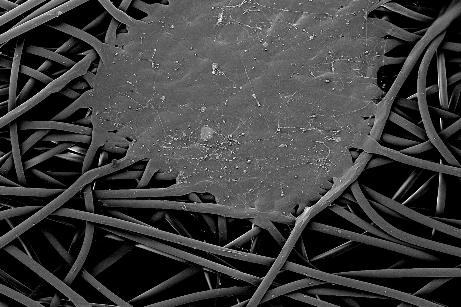
The ability to precisely analyze a material’s structure and composition at the microscopic scale is essential for advancing research and innovation. Scanning electron microscopy (SEM) has been a pivotal tool, providing high-resolution imaging of surface topography. Yet, imaging alone can only tell part of the story. To uncover the elemental makeup of these materials, scientists rely on energy dispersive X-ray spectroscopy (EDS), a powerful analytical technique integrated with SEM. EDS enables researchers to probe deeper, revealing not just how a material looks, but what it’s made of. Now, with advancements in SEM technology—particularly the Phenom Desktop SEM—this combination of imaging and elemental analysis is reaching new levels of speed and accessibility. Let’s explore what EDS offers and how the Phenom Desktop SEM is pushing the boundaries of material characterization.

What is Energy Dispersive X-Ray Spectroscopy (EDS)?
EDS is a technique commonly used in conjunction with SEM to determine which elements are present on the surface of a sample. The technique involves using an X-ray spectrometer to detect X-rays emitted from the sample while it is irradiated by the electron beam. Using specialized EDS software, the resulting X-ray spectrum can be analyzed to determine the relative elemental abundance at different points in the sample1, or to produce more sophisticated datasets like an elemental distribution map.
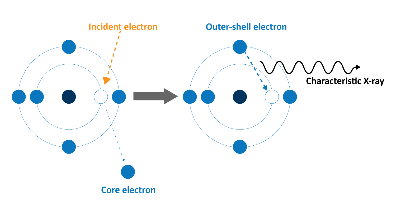
When the sample is exposed to the electron beam, different types of interactions occur between the incident electrons and atoms within the sample. Some of these interactions result in core-electrons being ejected due to inelastic scattering. As the ionized atom relaxes to a ground state, outer-shell electrons fill the empty core-hole, resulting in an X-ray being emitted with an energy equal to the difference between the two atomic energy levels (Figure 1). These so called “characteristic” X-rays, as seen as peaks in the EDS spectrum, are unique to the elements within the sample, providing a “fingerprint” that allows for precise identification. By measuring the energy of the emitted X-rays, EDS can determine the specific elements present and their relative abundance.2
What Can We Learn from SEM-EDS?
Combining SEM with EDS opens a world of information about a material’s composition. While SEM provides high-resolution images of surface morphology and topography, EDS adds an additional layer by revealing:
- Elemental Composition: Identifying which elements are present in a sample. EDS allows you to pinpoint the specific elements within a material by analyzing the unique X-rays emitted from the sample. This can reveal whether the sample contains elements such as carbon, oxygen, silicon, or metals like copper and gold. This is crucial for determining the raw materials or contaminants present in a wide range of applications, from metal alloys to biological samples.
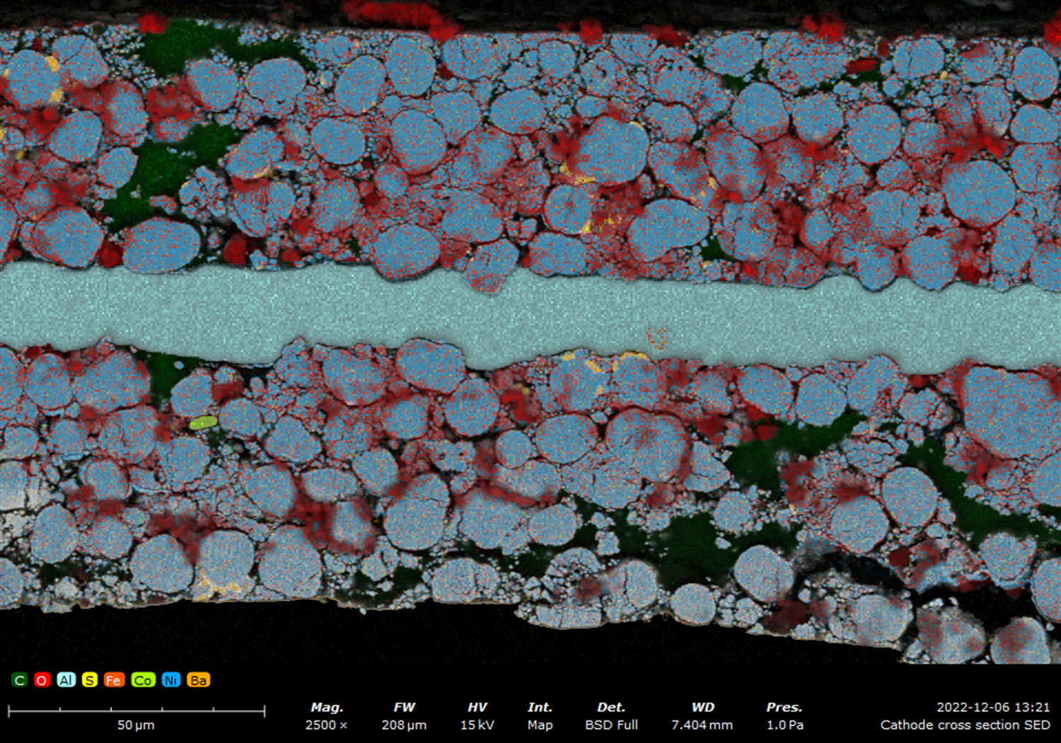
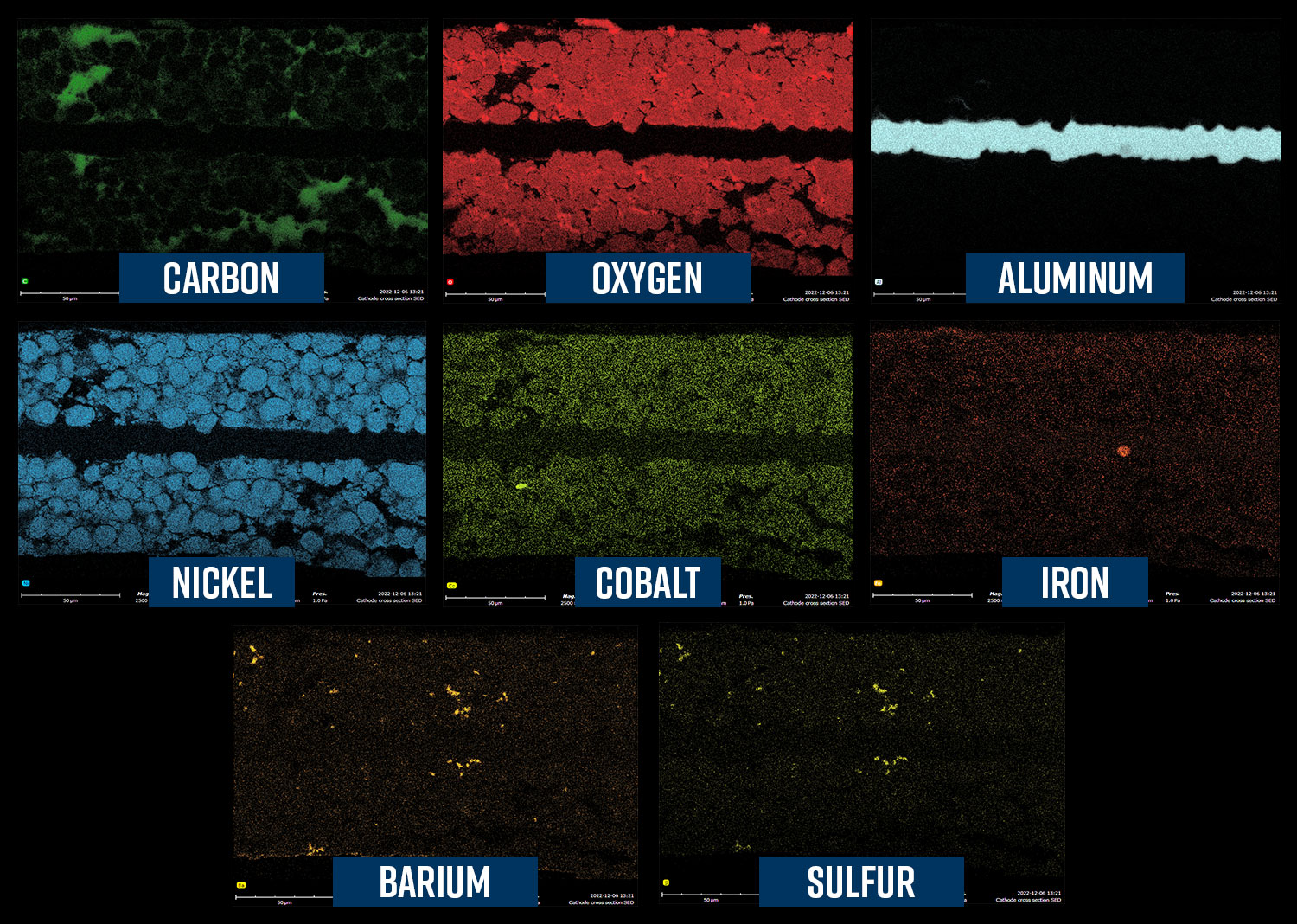
- Elemental Distribution: Mapping where specific elements are located across the surface. Beyond simply identifying elements, EDS can map the spatial distribution of each element over the sample’s surface. This reveals where certain elements are concentrated or how they are dispersed across different regions, which is particularly useful for detecting coatings, impurities, or variations in material composition. For example, in battery research, understanding how elements like nickel and cobalt are distributed across the electrode surfaces can inform performance and durability assessments (Figure 2).
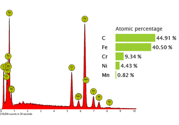
- Quantitative Analysis: Calculating the relative concentration of elements within a sample. EDS doesn’t just tell you which elements are present; it also provides a quantitative analysis of how much of each element exists in the sample (Figure 3). This is essential in industries where understanding localized composition is critical, such as alloy production, semiconductor manufacturing, and pharmaceuticals. Accurate elemental ratios are necessary to ensure product performance, compliance with material specifications, and quality control.
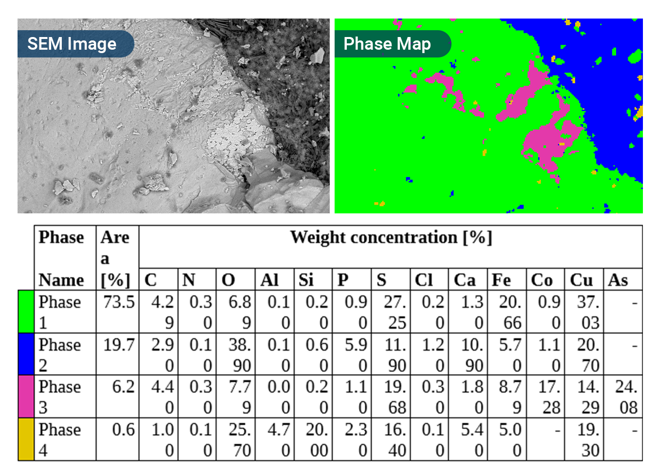
- Phase Analysis: Distinguishing different phases in a material by their elemental makeup. Many materials are composed of multiple phases, each with a distinct elemental composition. Dedicated analysis algorithms, when combined with SEM-EDS maps, can differentiate between these phases by identifying regions of similar composition. This is particularly important in materials like alloys, ceramics, or geological samples where different phases might contribute to unique mechanical or electrical properties. For example, in electronics, understanding the phases of a solder joint can help engineers assess its reliability (Figure 4).
Taking SEM-EDS to the Next Level with the Phenom Desktop SEM
Phenom Desktop SEMs takes SEM-EDS to the next level by providing seamless integration of imaging and elemental analysis in one compact system. The Phenom Desktop SEM sets new standards by:
- Ease of Use: Traditionally, SEM-EDS systems have been complex and required significant expertise to operate. The Phenom Desktop SEM simplifies this process with intuitive software and automated workflows, making high-quality analysis accessible to users of all experience levels.
- ChemiSEM Technology: The Phenom Desktop SEM features ChemiSEM technology, which enables real-time elemental mapping directly over the live SEM image. This provides a faster, more visual, and intuitive way to analyze the distribution of elements in your sample. The ability to perform chemical analysis while navigating across different regions of interest in real time is a game-changer for researchers.
- Phase Mapping: ChemiPhase (phase mapping) uses EDS data to distinguish and identify different phases within a sample. Unlike regular EDS mapping, which shows the spread of individual elements, phase mapping groups regions with similar elemental compositions into distinct clusters. This approach provides a deeper understanding of the sample’s microstructure by highlighting areas with similar elemental percentages, helping to identify different phases and offering valuable insights into the material’s properties and behavior.
- Speed and Efficiency: With a highly integrated system, users can go from imaging to full elemental analysis within minutes. This speed is particularly valuable in high-throughput environments like quality control labs, where rapid decision-making is essential.
- Compact and Accessible: Unlike conventional SEM-EDS systems that often require dedicated space and significant operational overhead, the Phenom Desktop SEM is compact and fits easily into any lab setting. This makes it a perfect choice for companies and research institutions seeking to enhance their analytical capabilities without the need for specialized infrastructure.
Conclusion
SEM-EDS is a vital tool for understanding the elemental composition and distribution of materials. The Phenom Desktop SEM not only offers best-in-class imaging with sub-micron resolution, but also integrates seamlessly with the EDS system for precise elemental identification. Whether you’re conducting research in material science, performing failure analysis, or optimizing battery technologies, the Phenom Desktop SEM with EDS capabilities is an essential tool for advancing your work.
To learn more about ChemiSEM and ChemiPhase, watch our on demand webinar “Enhancing Elemental Analysis with Real-Time Mapping: Phase Identification Using ChemiSEM & Phase Mapping”.
References
- D. E. Newbury and N. W. M. Ritchie, “Is Scanning Electron Microscopy/Energy Dispersive X-ray Spectrometry (SEM/EDS) Quantitative?,” The Journal of Scanning Microscopies, vol. 35, pp. 141-168, 2013. https://doi.org/10.1002/sca.21041 ↩︎
- J. I. Goldstein, D. E. Newbury, J. R. Michael, N. W. M. Ritchie, D. C. Joy and J. H. J. Scott, “Energy Dispersive X-ray Spectrometry: Physical Principles and User-Selected Parameters,” in Scanning Electron Microscopy and X-Ray Microanalysis, New York, NY, Springer, 2017, pp. 209-234. https://doi.org/10.1007/978-1-4939-6676-9_16 ↩︎