Energy Dispersive X-ray Spectroscopy (EDS) is an analytical technique used for elemental analysis and chemical characterization of materials. By detecting and measuring the energy of X-rays emitted from a sample when it is bombarded with high energy particles (such as electrons), EDS can determine the elemental composition of the material at a micro or nanoscale level. EDS is widely used in materials characterization because it allows for precise, localized analysis, making it essential for identifying impurities, understanding phase distributions, and analyzing complex multi-component systems. The data collected from EDS includes the energy and intensity of the detected X-rays, which are then used to generate spectra and elemental maps, revealing the spatial distribution of elements within the sample.
When coupled with scanning electron microscopy (SEM), EDS provides a non-destructive and comprehensive visualization of microstructure. In this blog, we dive into the basics of EDS and highlight several examples of how SEM-EDS is essential in materials science.

Characteristic X-rays
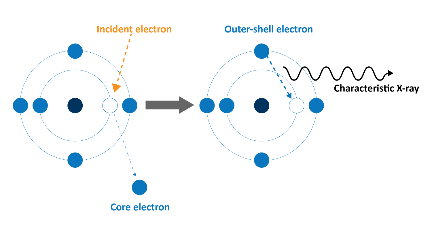
In the SEM, characteristic X-rays are generated when a material is irradiated by the high-energy electron beam (Figure 1). As the electron beam scans across the sample surface, incident electrons inelastically scatter with constituent atoms, causing bound (inner shell) electrons to be ejected and leaving behind a vacant energy level (core hole). An outer-shell electron then falls to this empty energy level, emitting an X-ray photon equal to the energy difference between the two energy levels. Since each element has unique atomic energy levels (and energy level differences), characteristic X-rays emission can be leveraged to identify what elements are present in a sample through EDS analysis.
Each element may have one or more transition energies that result in characteristic X-ray emission. Depending on the accelerating voltage of the SEM, which determines the incident electron energy, some transitions may not be excited. Therefore, it is important to consider the minimum accelerating voltage needed to excite characteristic X-ray emission in a sample when performing SEM-EDS. Typically, an accelerating voltage of at least 15 keV is used to include at least one characteristic X-ray elements.
The X-ray Spectrum
The EDS spectrum is a graphical representation of the X-ray energies detected during EDS analysis (Figure 2). It displays the intensity of the emitted X-rays as a function of their energy, with each peak corresponding to a specific element present in the sample. The intensity (and area) of these peaks indicates the abundance of the corresponding elements. Due to the transition energies involved, lighter elements’ characteristic X-ray peaks are located toward the low-energy side of the spectrum whereas heavier elements exhibit more numerous peaks that skew toward higher energies.
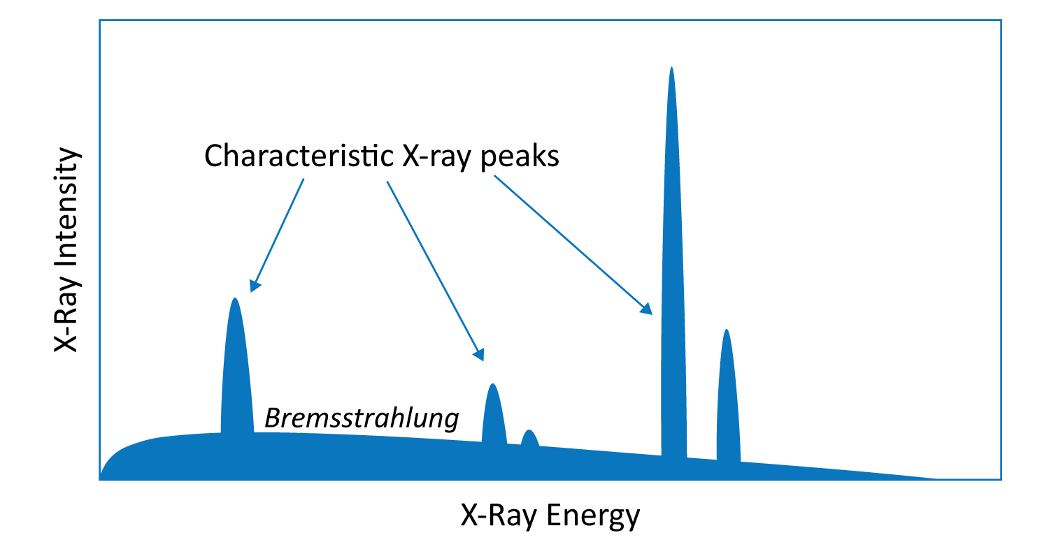
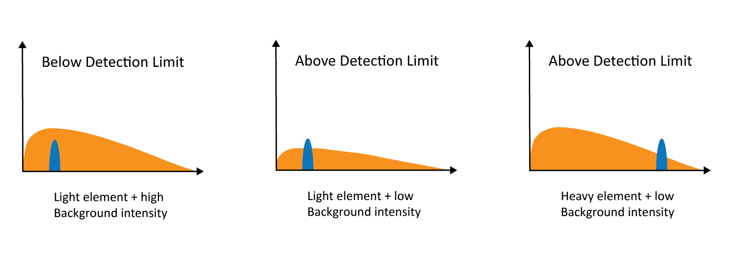
Bremsstrahlung (also known as “braking radiation”) creates a continuous X-ray background signal that obscures characteristic X-rays peaks. Braking radiation occurs when an incident electron is decelerated or deflected as it electrostatically interacts with atomic nuclei. This process causes the incident electron to lose energy in the form of an emitted X-ray. The amount of background radiation increases with the density of the sample, meaning that light elements in a heavy matrix can be difficult to detect (Figure 3).
Quantitative Analysis
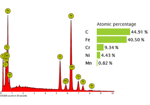
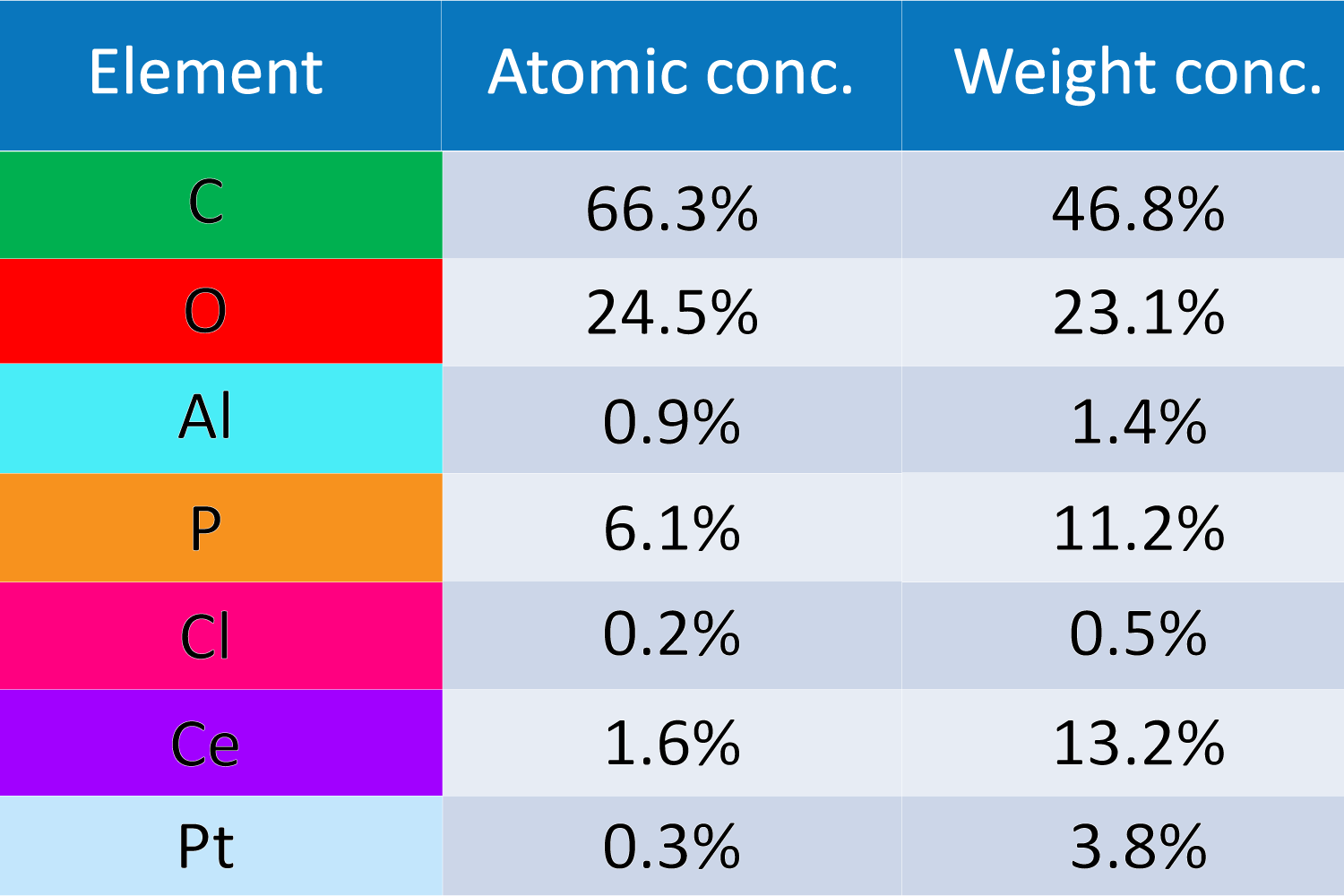
The X-ray spectrum can be used for quantitative analysis by measuring the intensity of characteristic X-ray peaks corresponding to different elements in the sample. An example of quantitative analysis is shown in Figure 4. The steps involved in using the X-ray spectrum for quantitative analysis are as follows:
Peak Identification: The first step is identifying the characteristic peaks in the EDS spectrum, which correspond to specific elements. EDS analysis software can be used to automatically identify peaks and accurately deconvolute overlapping peaks using linear least-squares fitting methods of reference peaks.
Background Subtraction: The continuous background, to bremsstrahlung radiation, is subtracted from the spectrum to accurately measure the peak intensities. This ensures that only the characteristic X-ray peaks are considered in the analysis.
Peak Intensity Measurement: The integrated intensity (area) of these characteristic peaks is calculated. The intensity is directly related to the abundance of the corresponding elements in the sample.
Standardization and Calibration: Quantitative analysis often requires calibration with standards of known composition. These standards help in determining the efficiency of the detector and the system’s response to different elements.
Matrix Effects Correction: Corrections are applied to account for matrix effects, which include absorption and fluorescence effects that can alter the detected intensity of X-rays. These corrections ensure that the measured intensities accurately reflect the actual concentrations of elements.
Quantitative Calculation: Using the corrected peak intensities and calibration data, the concentration of each element in the sample is calculated. This can be done using various quantitative algorithms and software provided with the EDS system.
Examples of EDS in Materials Science
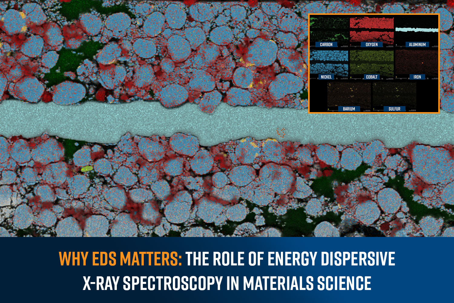
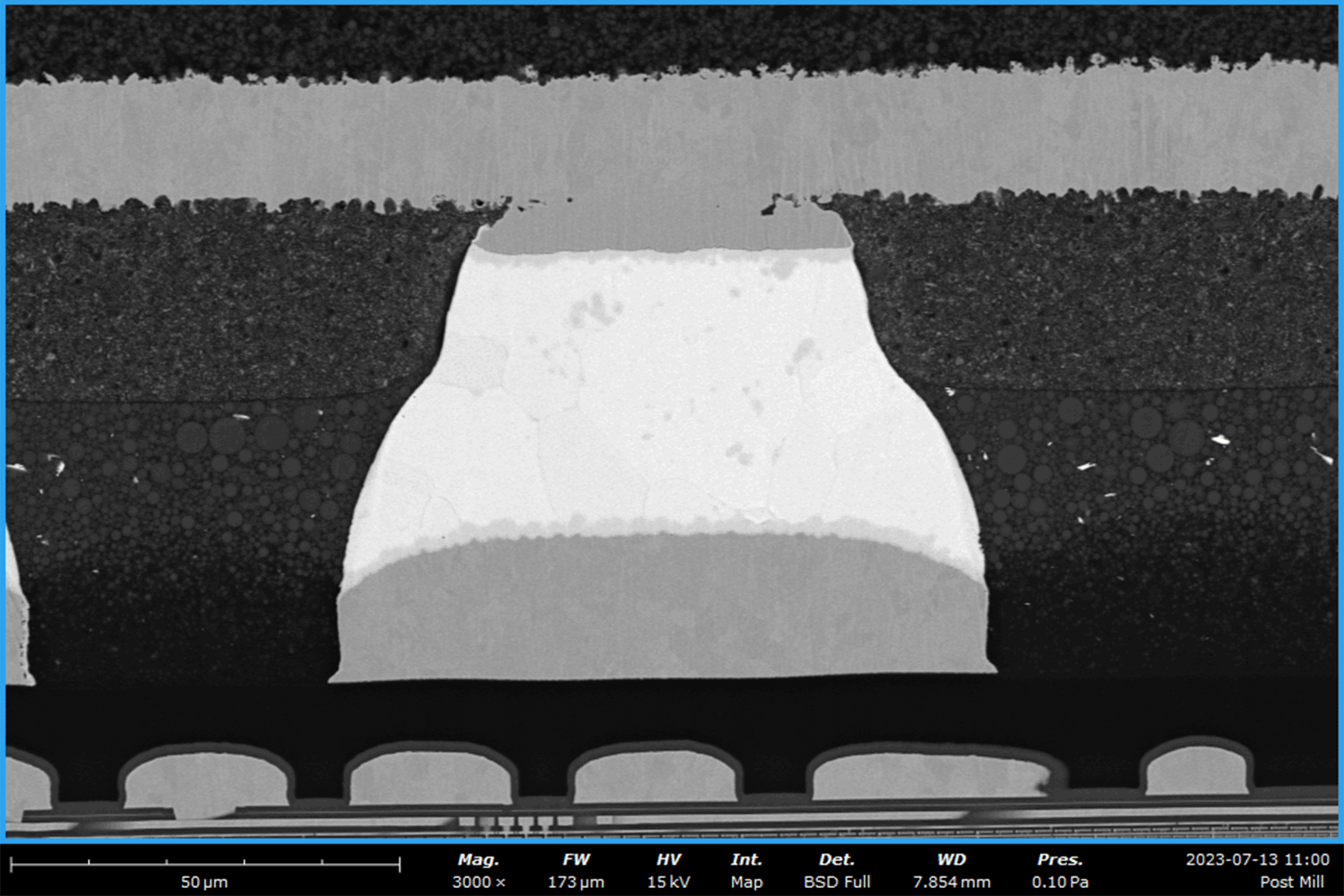
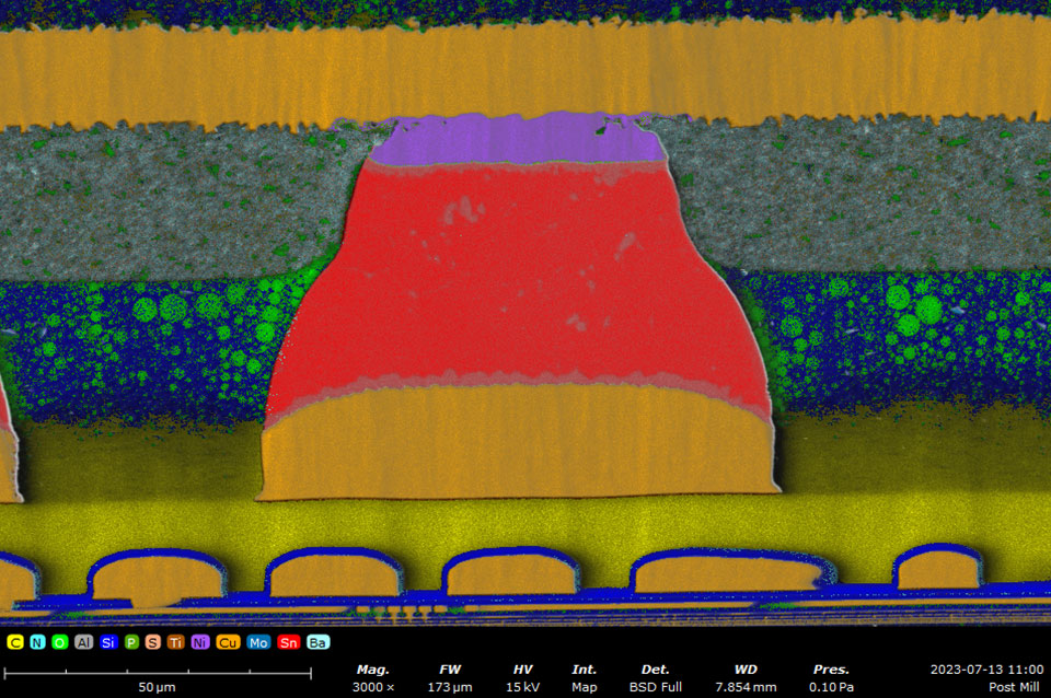
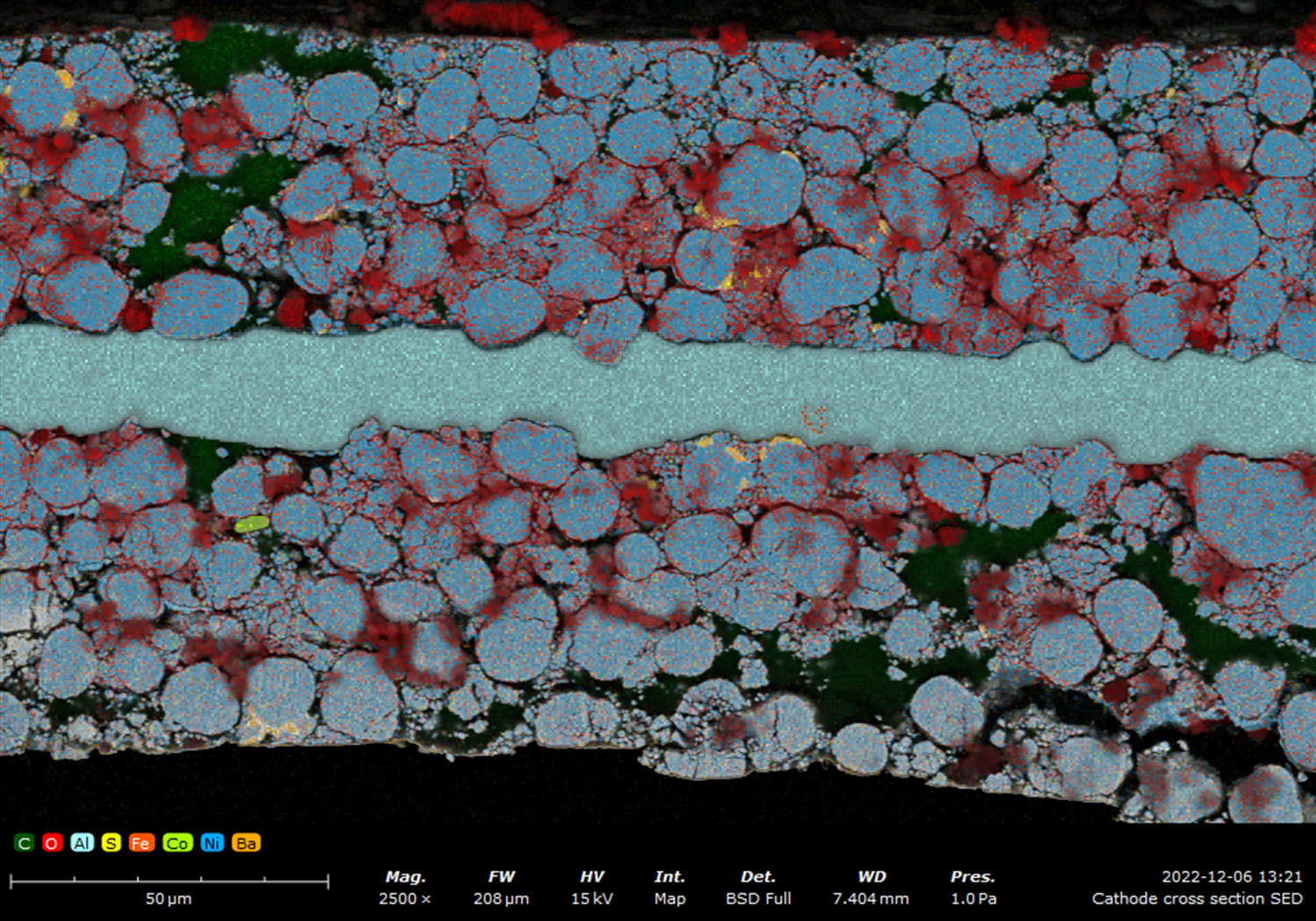
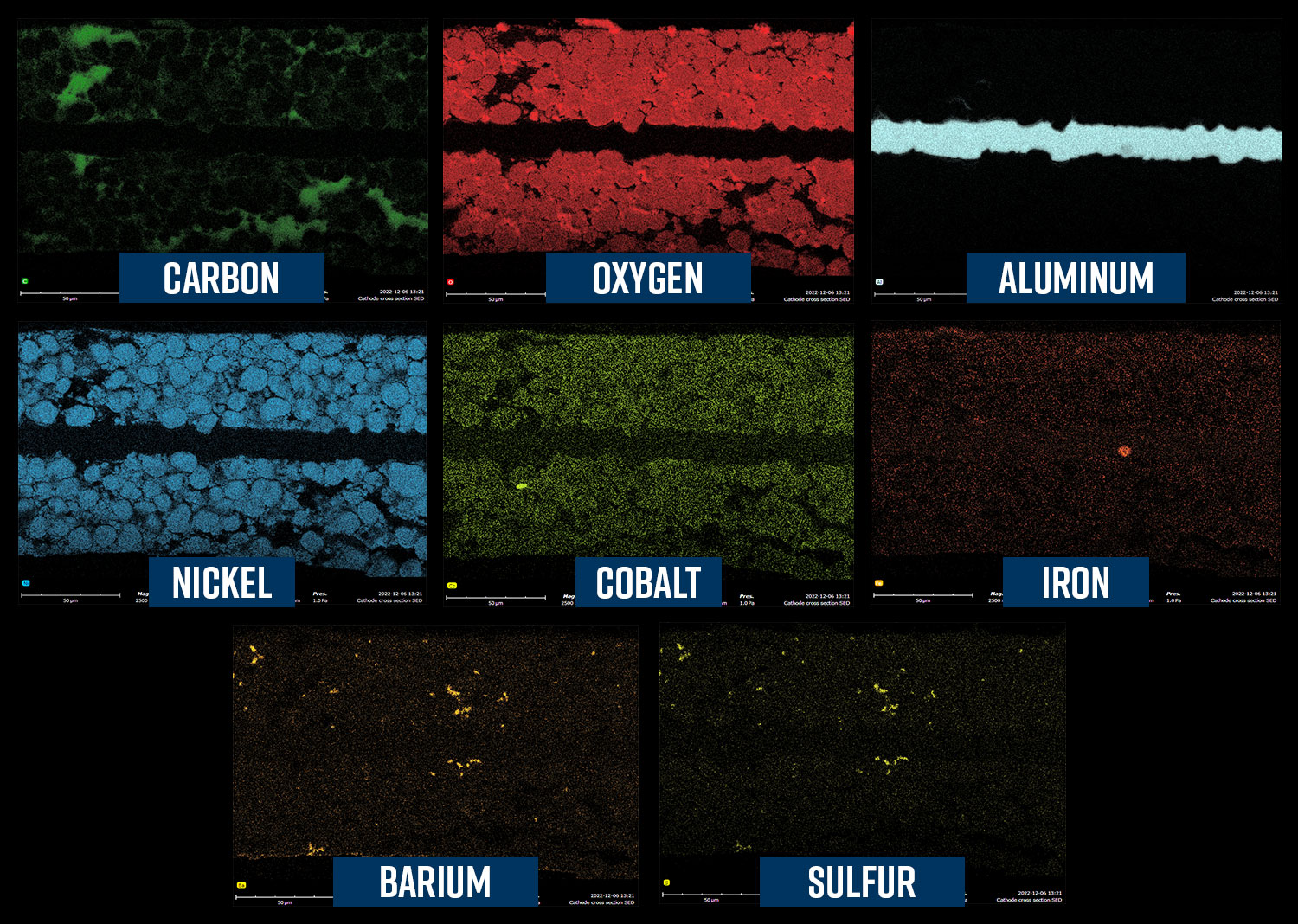
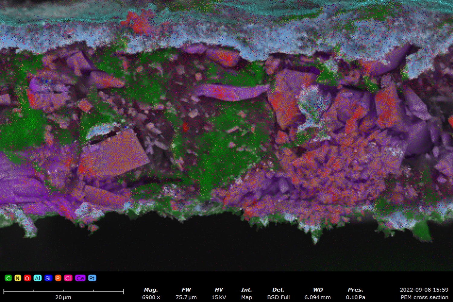
SEM-EDS allows for localized analysis of elemental composition, providing detailed insights into the microstructure of materials and devices. One of the most valuable types of data that SEM-EDS can provide is elemental abundance maps. EDS maps provide a false color visualization of one or multiple elements’ distribution within a sample. Combined with quantitative analysis, SEM-EDS is routinely used in a wide range of applications, including the following:
Semiconductor packaging
SEM-EDS analysis is used in semiconductor packaging development for its ability to aid in failure analysis by detecting contaminants and analyzing device failures. Routine EDS analysis is part of the quality control process to ensure that the materials and processes used in semiconductor packaging meet the required specifications. It helps in detecting deviations in material composition or process parameters early, allowing for corrective actions.
Batteries
In battery development, EDS helps in identifying and optimizing the materials used for electrodes, enhancing battery performance and longevity by analyzing the distribution and concentration of active elements.
Fuel Cells
For fuel cells, EDS is critical in studying catalyst materials, allowing for the improvement of efficiency and durability by understanding the elemental makeup and distribution of the catalysts.
Key Takeaways
SEM-EDS is a non-destructive technique that involves analyzing X-rays emitted from the sample while it is being irradiated by the electron beam. In this way, localized analysis of a sample’s composition can be obtained and correlated to topographical SEM images. Quantitative analysis involves analyzing the background-subtracted intensity of characteristic X-ray peaks and making necessary corrections for matrix effects and calibration with standards. Using EDS in materials science has significant implications across various domains, enhancing the understanding, development, and optimization of materials.