Recent advancements in food science research represent a dynamic frontier with profound implications for our global food systems. Breakthroughs in food preservation and packaging technology…
Posted: February 8, 2024

Contact angle is defined as the angle formed by a liquid at the three-phase boundary where the liquid, solid, and gas intersect. It gives a…
Posted: February 7, 2024
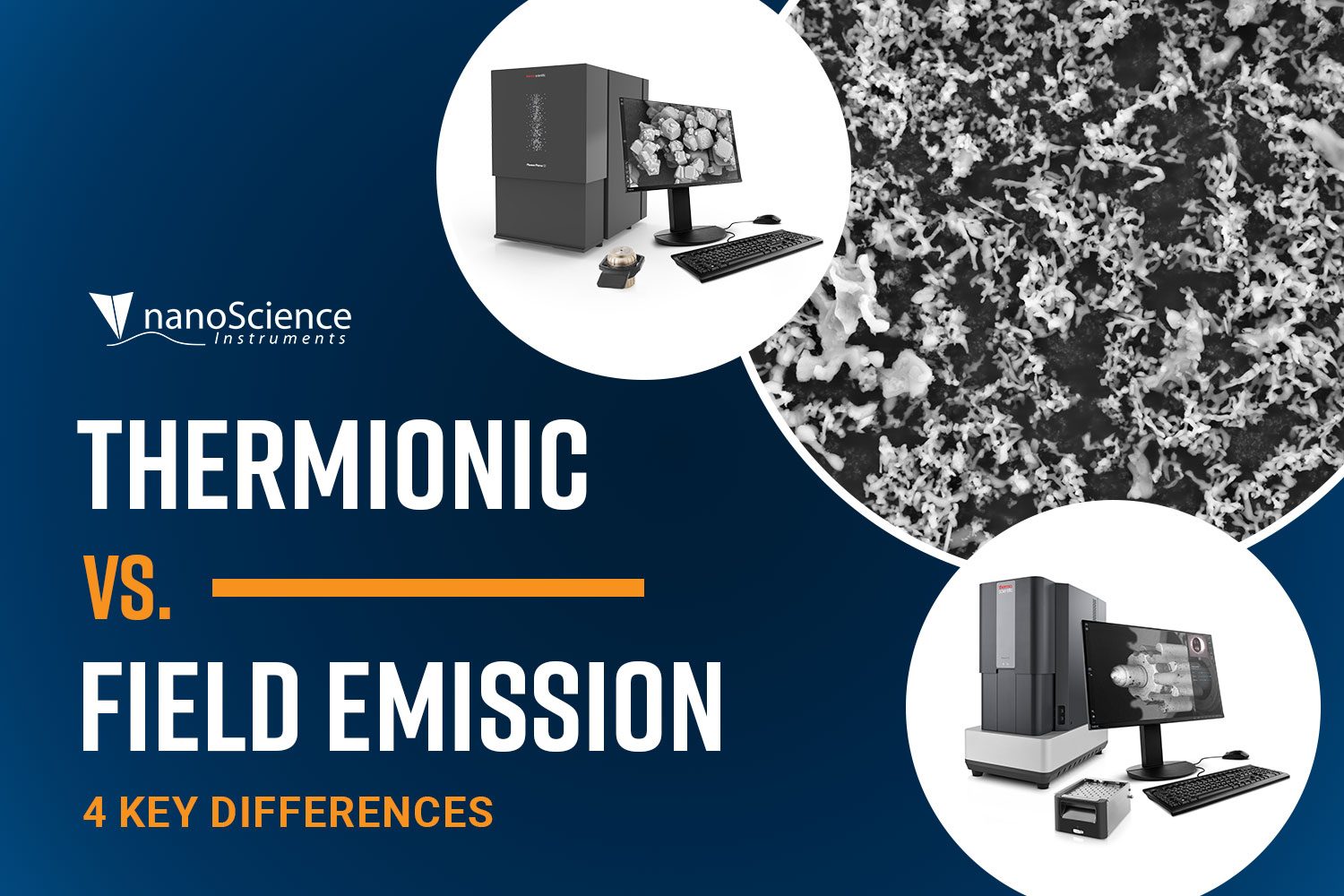
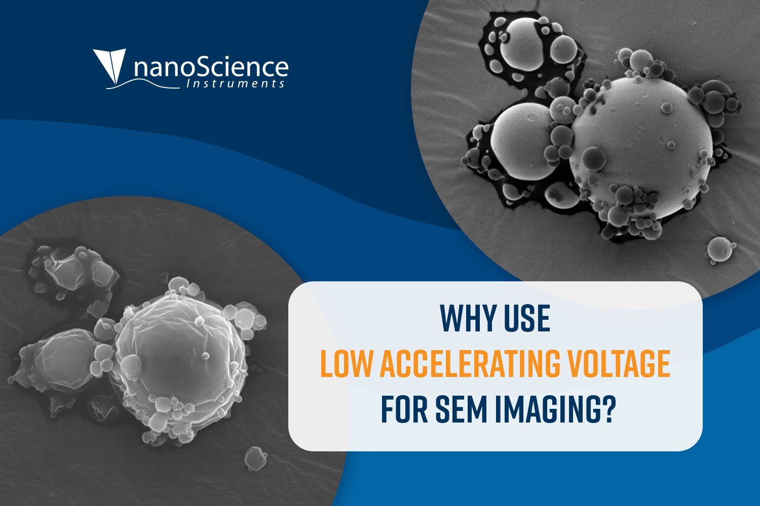
The electron source is one of the most critical components of a scanning electron microscope (SEM) because it determines the quality, brightness, and size of…
Posted: January 31, 2024
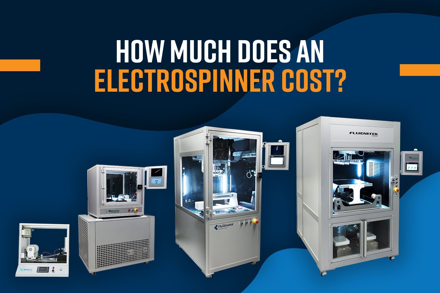
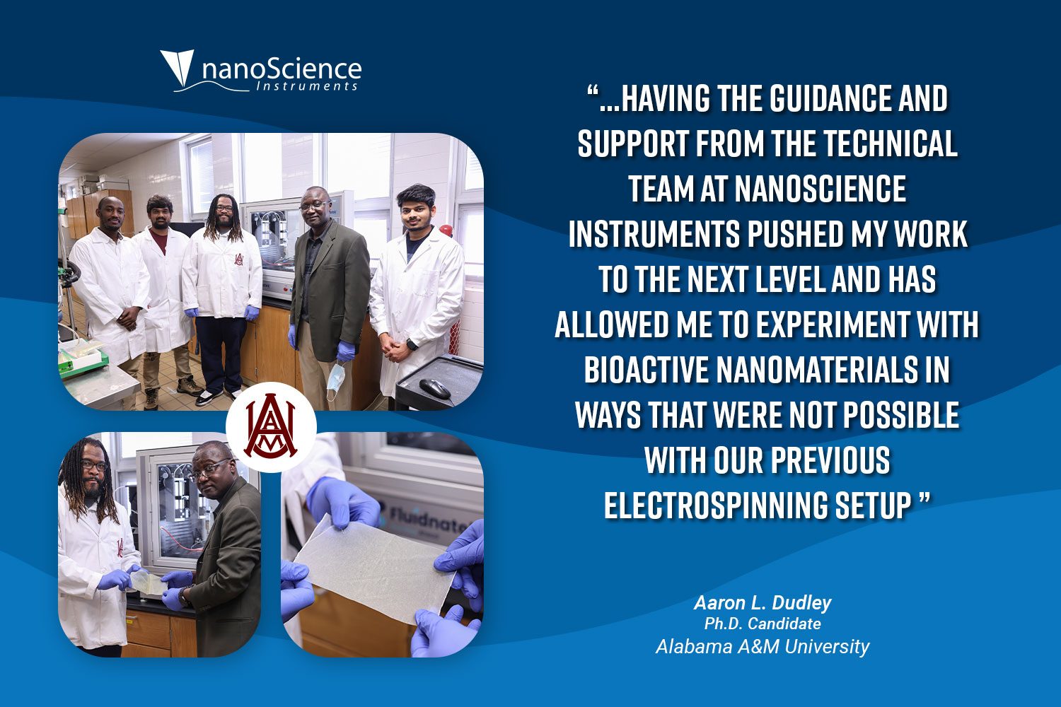
Electrospinning and electrospraying technologies continue to gain prominence due to their versatility in nanofiber and nanoparticle development. Researchers, scientists, entrepreneurs, and industry professionals face the…
Posted: January 17, 2024

MD&M West – Medical Design & Manufacturing West Learn More Nanoscience Instruments and our sister company, Nanoscience Analytical, provide cutting-edge instrumentation and process development services…
Posted: January 11, 2024

Biophyisical Society 2024 Annual Meeting Learn More Stop by to explore our sample preparation solutions for streamlining your structural biology research workflows. The VitroJet helps…
Posted: January 11, 2024
In this Electrospinning edition of our newsletter, we introduce you to the unique technology behind Fluidnatek’s new LE-500 BioDevice Electrospinning & Electrospraying system and provide…
Posted: January 10, 2024
Electron microscopy is best known as a high-powered microscopy technique that utilizes a beam of electrons as a source of illumination. In an electron microscope,…
Posted: January 10, 2024

In this Tensiometry edition of our newsletter, we provide you with new application notes, webinars, and blog posts that explore contact angle misconceptions, wettability of…
Posted: January 4, 2024
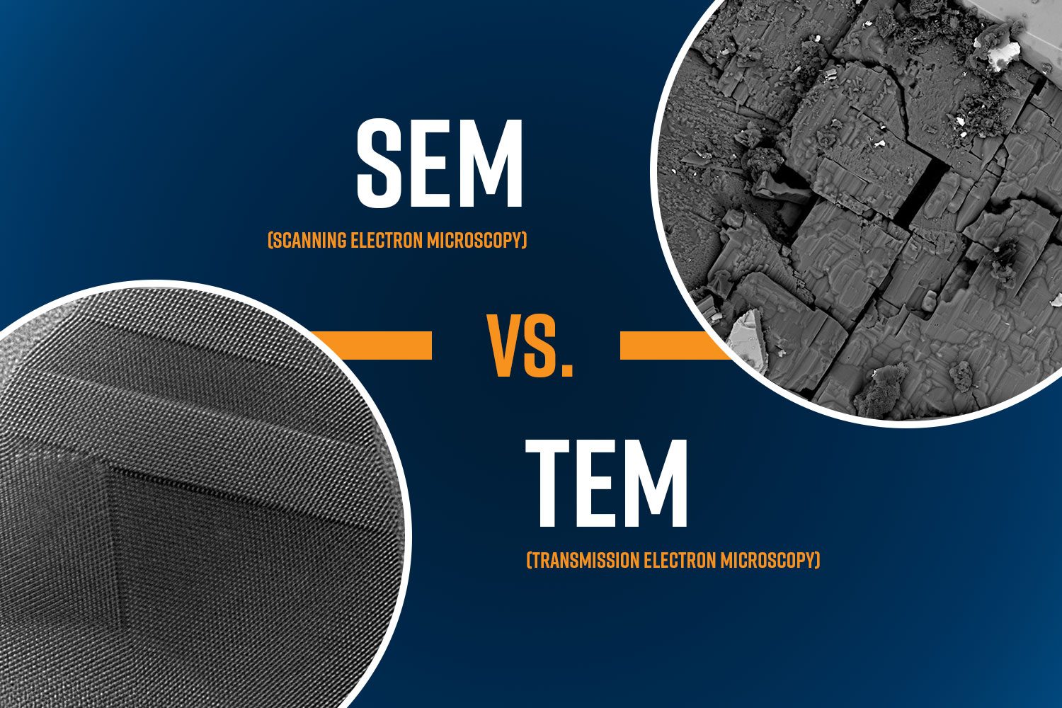
Scanning electron microscopes (SEM) function by rastering a sample with a focused beam of electrons to produce high-resolution images of the sample surface. The generated…
Posted: January 3, 2024

SEM is a high-resolution imaging technique that uses a focused electron beam to generate high-resolution images of the surface morphology and the elemental composition of…
Posted: December 27, 2023
Nanofibers, particularly polymeric nanofibers, are a burgeoning frontier in the world of materials science, offering a diverse array of applications across industries. These fibers, typically…
Posted: December 20, 2023
Copyright 2025. Nanoscience Instruments. All Rights Reserved.
This site is protected by reCAPTCHA and the Google Privacy Policy and Terms of Service apply.