
We’re pleased to share the latest edition of nanoNews! In this first quarter newsletter, you’ll find our webinar resources, event news, and our newest articles and technical notes — all focused on Scanning Electron Microscopy (SEM).
UPCOMING EVENT

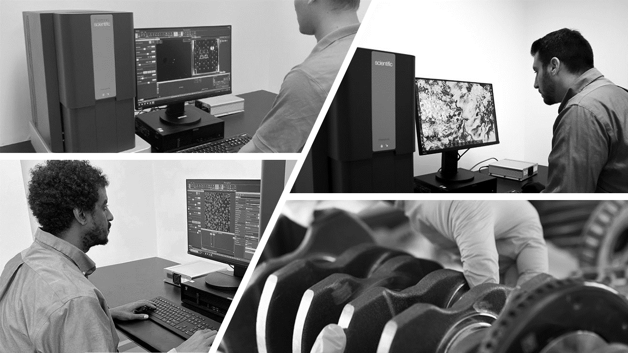
Join us at the Association for Iron & Steel Technology show in Columbus, OH this May! Our SEM experts will showcase the ParticleX Steel SEM/EDS system designed for automated inclusion imaging and compositional analysis. Contact us for a free expo pass!

NEW TECH NOTES & BLOGS
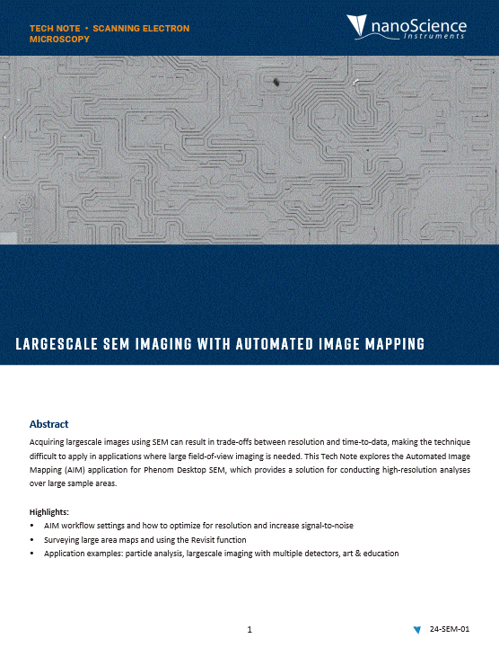
Large-scale SEM Imaging with Automated Image Mapping
With Automated Image Mapping (AIM), define a zone and field width, among other parameters, to produce a seamless, comprehensive mosaic of hundreds of high resolution SEM images. Hours (if not days) of work transform into mere minutes.
With this high resolution micrograph map, you are then able to survey vast areas and revisit features of intrigue in more detail. Check out the technical note to learn more and see AIM examples!
What are the Pitfalls of Neglecting Technical Cleanliness Standards?

Precision manufacturing is a process that emphasizes exact specifications and extremely tight tolerances within fabricated components. Within this domain, the term technical cleanliness (TC) refers to the rigorous control of …
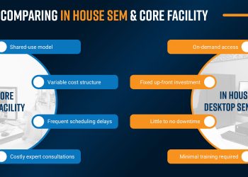
In-House or Core Facility SEM: Which Path is Right for You?
Scanning electron microscopy (SEM) is an essential tool that allows scientists to directly visualize the surface structure and composition of a variety of materials on the nanometer to micrometer scale. …
6 Applications of SEM & EDS in Pharmaceutical Sciences

In the evolving landscape of pharmaceutical research and development, the goal to understand the micro and nanoscale properties of therapeutics is vital. Central to this pursuit is the deployment of …
Understanding the Difference between Magnification and Resolution in Scanning Electron Microscopy

Microscopes have revolutionized our ability to observe and analyze the microscopic world with unprecedented detail. By enlarging our view of objects, or magnifying them, microscopes allow us to visualize a …
What’s the Difference Between SEM & TEM?
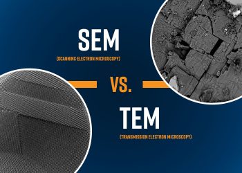
Electron microscopy is best known as a high-powered microscopy technique that utilizes a beam of electrons as a source of illumination. In an electron microscope, a focused electron beam interacts …
Thermionic vs. Field Emission Sources: 4 Key Differences

The electron source is one of the most critical components of a scanning electron microscope (SEM) because it determines the quality, brightness, and size of the electron beam used for …
Four Benefits of SEM Automation for Handling Repetitive Tasks

SEM is a high-resolution imaging technique that uses a focused electron beam to generate high-resolution images of the surface morphology and the elemental composition of specimens at a micro- and …
Why Use Low Accelerating Voltage for SEM Imaging?
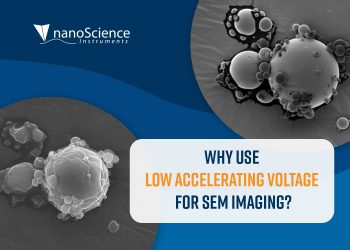
Scanning electron microscopes (SEM) function by rastering a sample with a focused beam of electrons to produce high-resolution images of the sample surface. The generated signals from these sample-beam interactions …