
We’re pleased to share the latest edition of nanoNews! In the second quarter newsletter, you’ll find our webinar resources, event news, and our newest articles and technical notes — all focused on Scanning Electron Microscopy (SEM).
NEWS & UPDATES
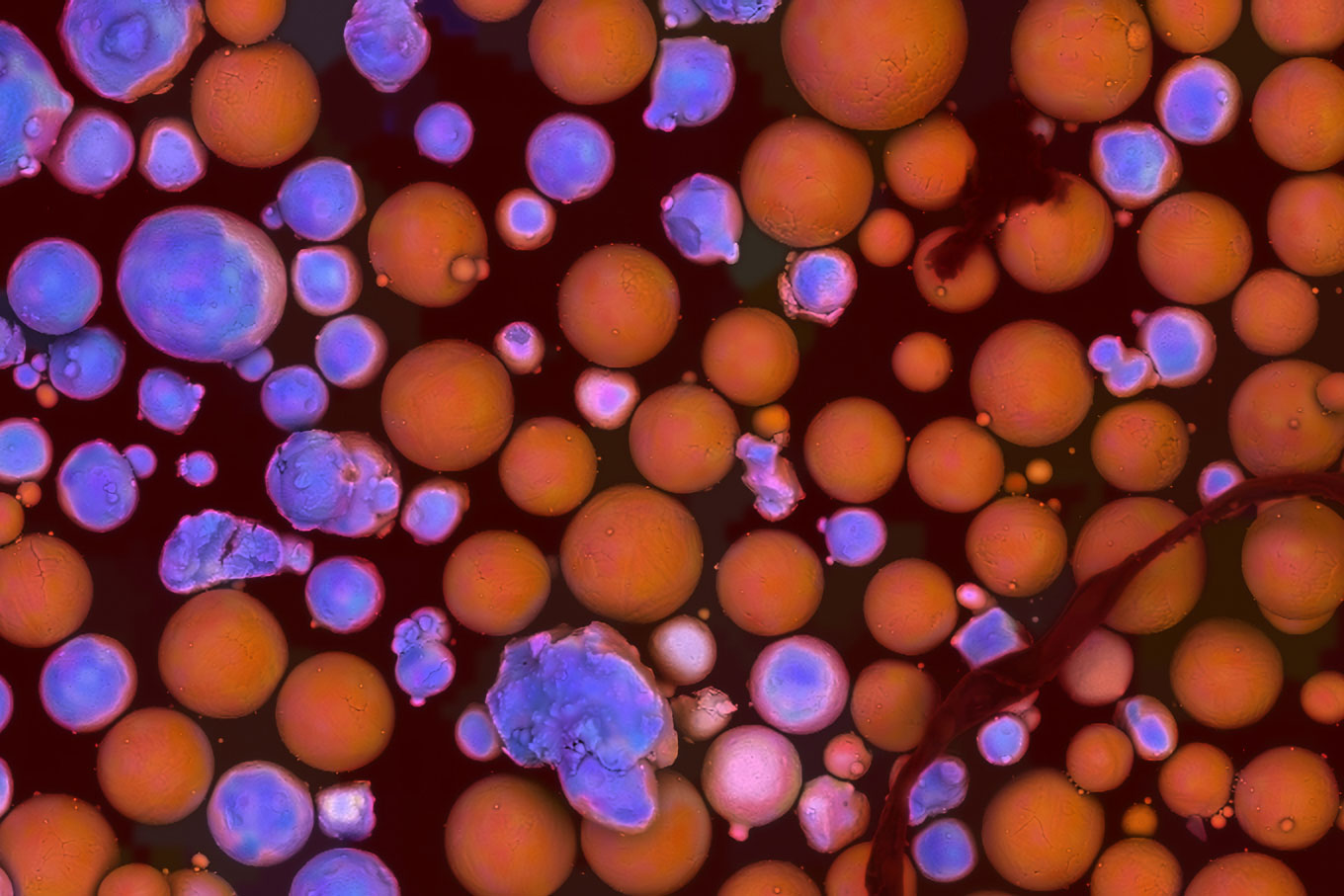
NEW EDS CAPABILITIES
Live Quantitative Elemental Mapping
ChemiSEM brings chemical compositions to live SEM imaging on the same screen. This software ensures X-rays are continuously detected during imaging, creating distinct color-coded overlays.
WEBINAR RECORDINGS
CONFERENCE CORNER
UPCOMING EVENT
Microscopy and Microanalysis 2024

Join us at this year’s Microscopy and Microanalysis (M&M) event! To learn more about
the show, sign up for product demos, and more, view the details on our website here:

TECH NOTES & BLOGS
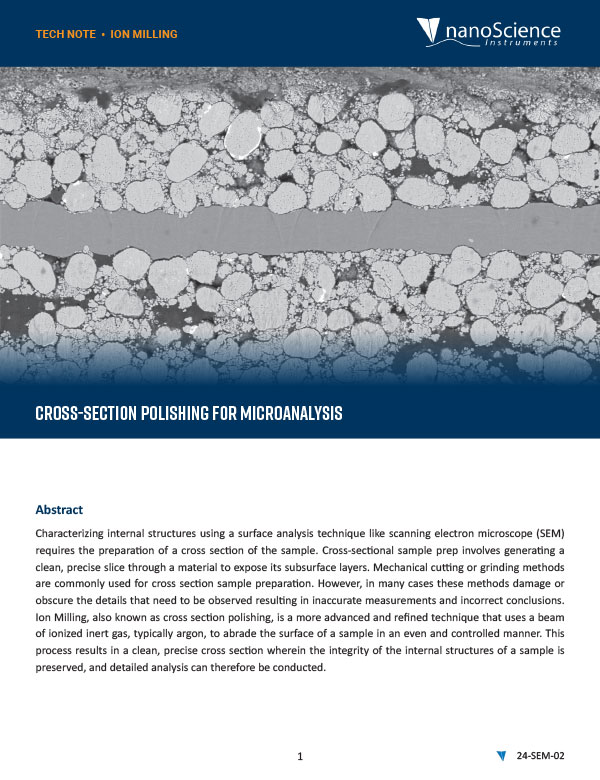
TECH NOTE
Cross-Section Polishing for Microanalysis
Explore how cross-sectional analysis in scanning electron microscopy reveals the internal structures of layered and complex materials. Ion milling, a technique used for polishing cross-sections with control and precision, is vital in industries with materials like electronics, batteries, and semiconductors.
BLOGS:
Struck by an Electron Beam: Interactions at the Surface in SEM
Scanning Electron Microscopy (SEM) is one of the most important tools in the arsenal of modern material science used to characterize micro and nanoscale features. Central to its functionality is …
Improving Microstructural Analysis in SEM Imaging with Gamma Correction
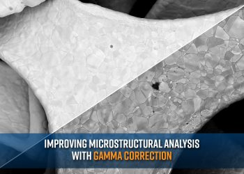
A scanning electron microscope (SEM) is capable of visualizing compositional heterogeneity on the surface of a sample by employing a backscattered electron detector (BSD). A BSD works by detecting elastically …
SEM Imaging of Uncoated, Nonconductive Samples
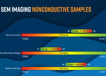
Scanning Electron Microscopy (SEM) generates high-resolution images by scanning a focused beam of electrons across the sample surface and detecting the signals produced through beam-sample interactions. Imaging nonconductive samples by …
What is Technical Cleanliness?

Technical cleanliness is an analytical standard to determine the level of particulate contamination on machined parts. The goal of technical cleanliness is to characterize the particles on the components and …
How Does Coating Thickness Affect SEM Imaging?
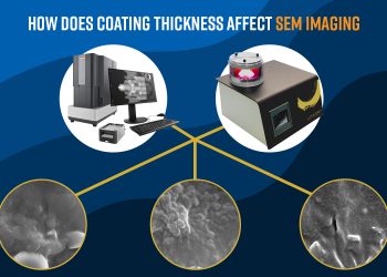
Charging is one of the most common issues when imaging non-conductive samples by scanning electron microscope (SEM) as it can distort images and damage the sample. Sputter coating samples can …
Gold vs Platinum: Choosing the Right Coating for SEM Imaging

One of the most common challenges when analyzing non-conductive samples with a scanning electron microscope (SEM) is the charging effect. Without a conductive path, the electrons accumulate at the surface, …
Infrastructure Essentials: Preparing Your Workspace for a Phenom Desktop SEM

Integrating the ability to perform high-resolution imaging and compositional analysis of materials into any laboratory becomes simplified with a desktop scanning electron microscope (SEM). In addition to the compact footprint, …
Cutting Costs, Not Corners: Why Phenom Desktop SEMs are a Smart Investment
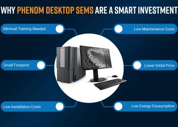
When acquiring a new scanning electron microscope (SEM), it can be challenging to identify a solution that not only delivers exceptional performance but also remains financially feasible. Among the myriad …