We’re excited to share the latest edition of SEM nanoNews with you! You’ll find updates on Phenom software, new additions to our website, and everything you need to know about upcoming events, webinars, blogs, and our expanded image gallery—all centered around Scanning Electron Microscopy (SEM).
Don’t miss out- Follow us on LinkedIn to stay up to date on news, publications and more!

NEWS & UPDATES
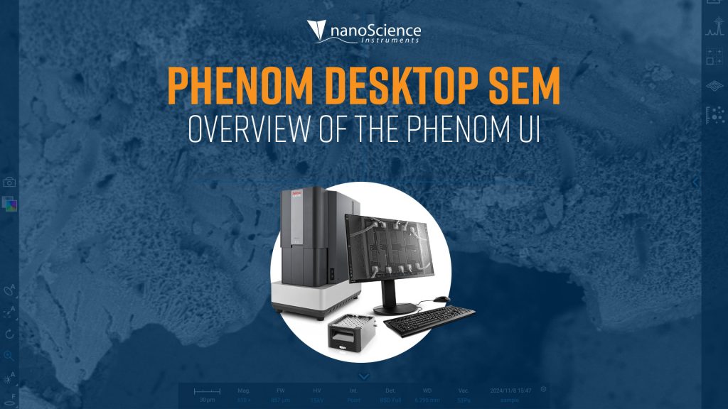
NEW VIDEO – OVERVIEW OF THE PHENOM UI
Live SEM images, an optical overview, clean menus, and straightforward controls culminate into an accessible and intuitive, friendly user experience.
AVIZO TRUEPUT
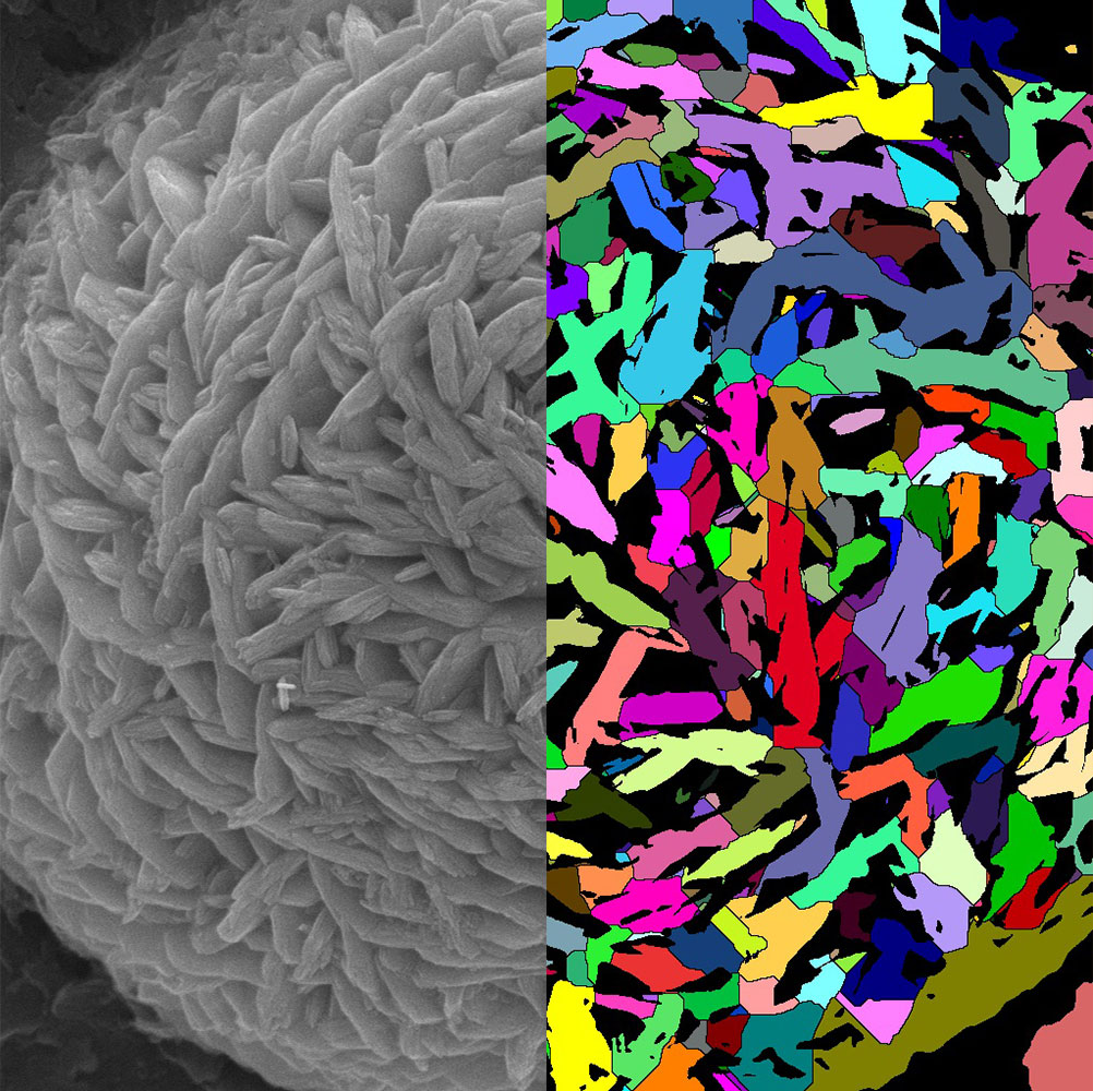
Avizo Trueput is a dedicated battery quality analysis software designed to streamline battery inspection on the production floor. It converts SEM image datasets into clear, reproducible pass/fail reports. This powerful tool enables QA/QC teams to maximize efficiency and maintain quality standards.
CONFERENCE CORNER
UPCOMING EVENTS:
MD&M WEST 2025

Stop by our booth #541 at Medical Design & Manufacturing West to explore how our advanced microscopy solutions can enhance your material analysis. Experience the best-selling Phenom Desktop SEM firsthand, equipped with ChemiSEM technology that lets you visualize both sample morphology and elemental distribution simultaneously, delivering fast and actionable insights.

WEBINARS
Thursday, January 30th 2025 – 12 PM Eastern
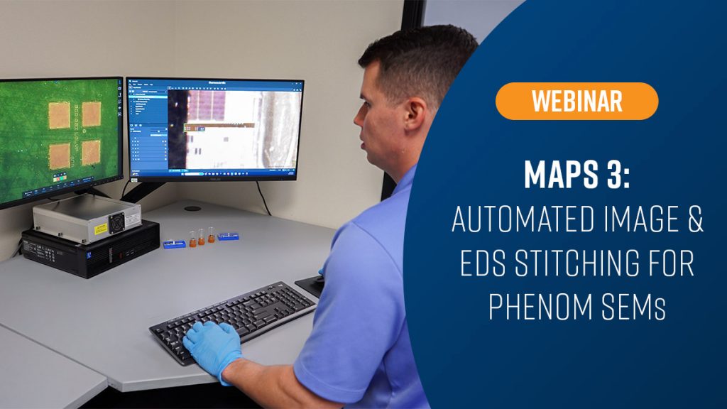
In our upcoming webinar, Application Scientist Ron Allen will showcase the powerful features of MAPS 3 and provide practical tips that will help elevate your facility’s SEM imaging capabilities. Discover how MAPS 3 is ideal for both novice microscopists and experienced researchers, delivering precision, versatility, and significant time savings.
Available On Demand:
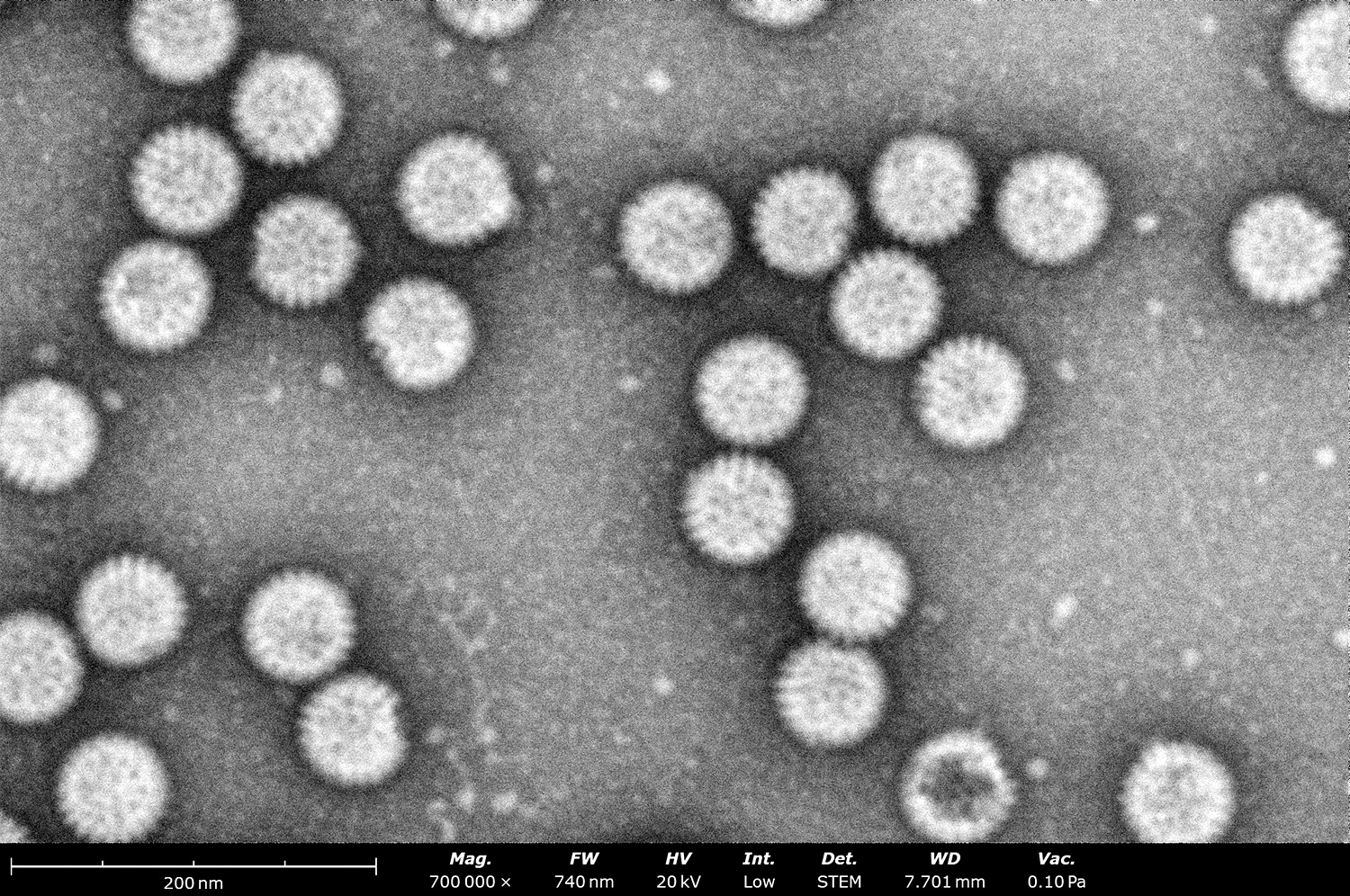
Enhancing Cryo-TEM Efficiency: Screening Negatively Stained Samples with Desktop STEM
Negative Stain imaging is a critical step in the single-particle cryo-EM workflow, allowing researchers to assess sample quality at room temperature before moving to complex cryo-preparation and imaging. Traditionally, this …
The Latest with Phenom SEMs: New Updates and Analysis Software
You are invited to an exclusive webinar where we will showcase the latest software release for Phenom SEM. During the session, Dr. Vince Pastore, Phenom Product Manager and Application Scientist, …
Enhancing Elemental Analysis with Real-Time Mapping: Phase Identification Using ChemiSEM & Phase Mapping
Elemental analysis is a crucial aspect of material characterization, but traditional methods can be time-consuming and complex. ChemiSEM revolutionizes this process by utilizing machine learning and ultrafast signal processing to …

BLOGS
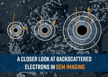
A Closer Look at Backscattered Electrons in Scanning Electron Microscopy (SEM) Imaging
Materials scientists leverage a range of advanced analytical techniques to extract detailed information regarding a sample’s structure, properties, and defects. Scanning electron microscopy (SEM) is a cornerstone of these methods, …
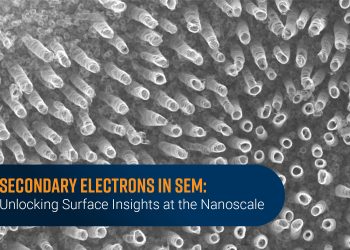
Secondary Electrons in SEM: Unlocking Surface Insights at the Nanoscale
In scanning electron microscopy (SEM), secondary electrons (SE) play a pivotal role in revealing the surface details of materials at the nanoscale. Understanding what secondary electrons are, how they are …
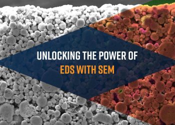
Unlocking the Power of Energy Dispersive X-Ray Spectroscopy (EDS) with Scanning Electron Microscopy (SEM)
The ability to precisely analyze a material’s structure and composition at the microscopic scale is essential for advancing research and innovation. Scanning electron microscopy (SEM) has been a pivotal tool, …
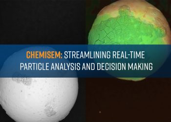
ChemiSEM: Streamlining Real-Time Particle Analysis and Decision Making
Energy dispersive spectroscopy (EDS) is a microanalysis technique that provides localized elemental composition data, typically used in conjunction with scanning electron microscopy (SEM). While SEM-EDS can provide elemental composition at …
SEM Characterization of Recycled Materials for the Circular Economy
In the age of climate change and resource depletion, the circular economy is increasingly gaining attention. It promotes the reuse, recycling, and repurposing of materials to create sustainable production and …

