

PHENOM DESKTOP SEM
Electron Sources
Phenom Desktop SEMs are equipped with two advanced electron source options, each tailored to specific imaging needs. The Cerium Hexaboride (CeB6) crystal is a thermionic electron source, while the Schottky Field Emission Gun (FEG) relies on electron tunneling.
High-Quality Imaging
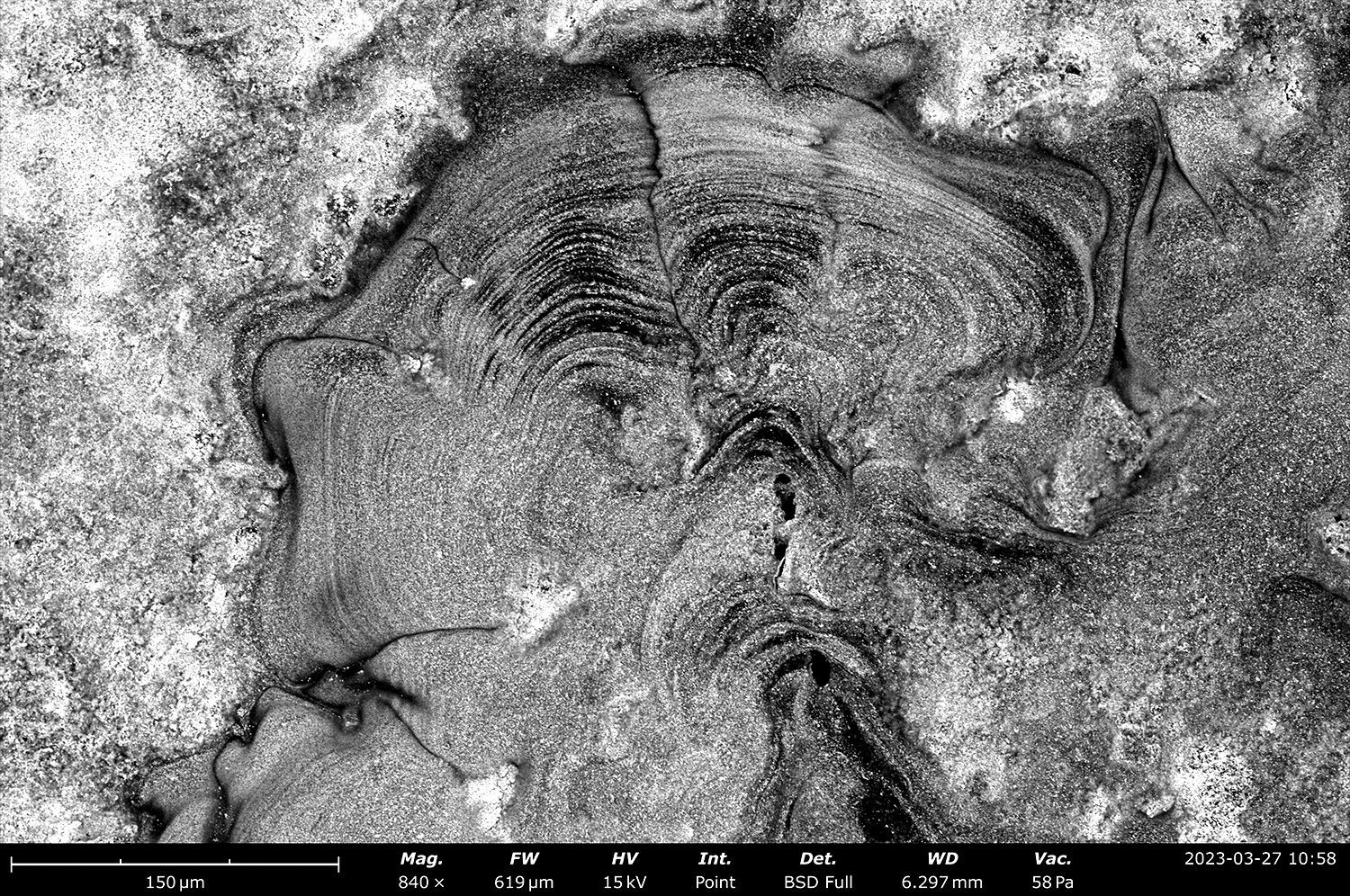
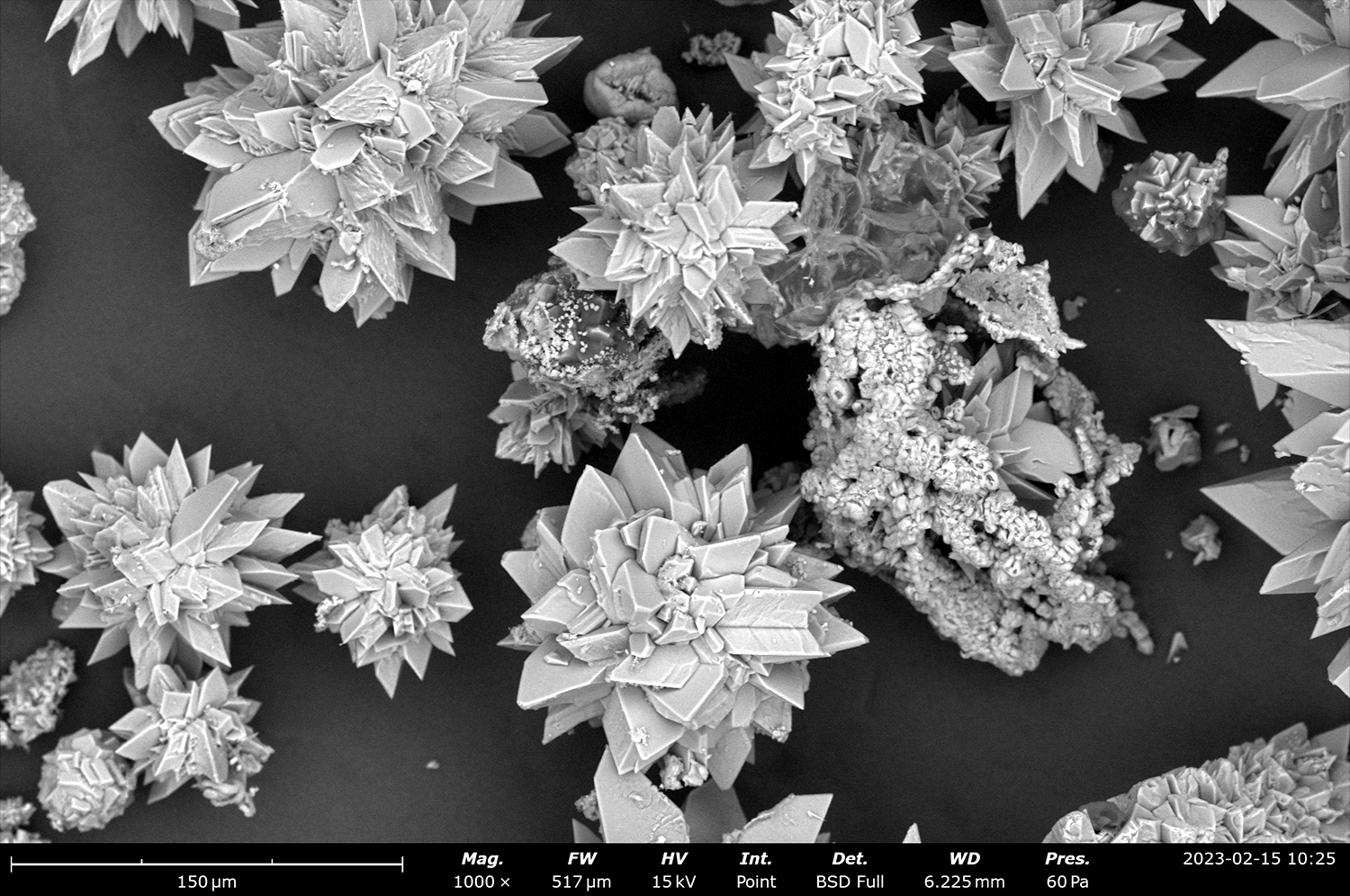
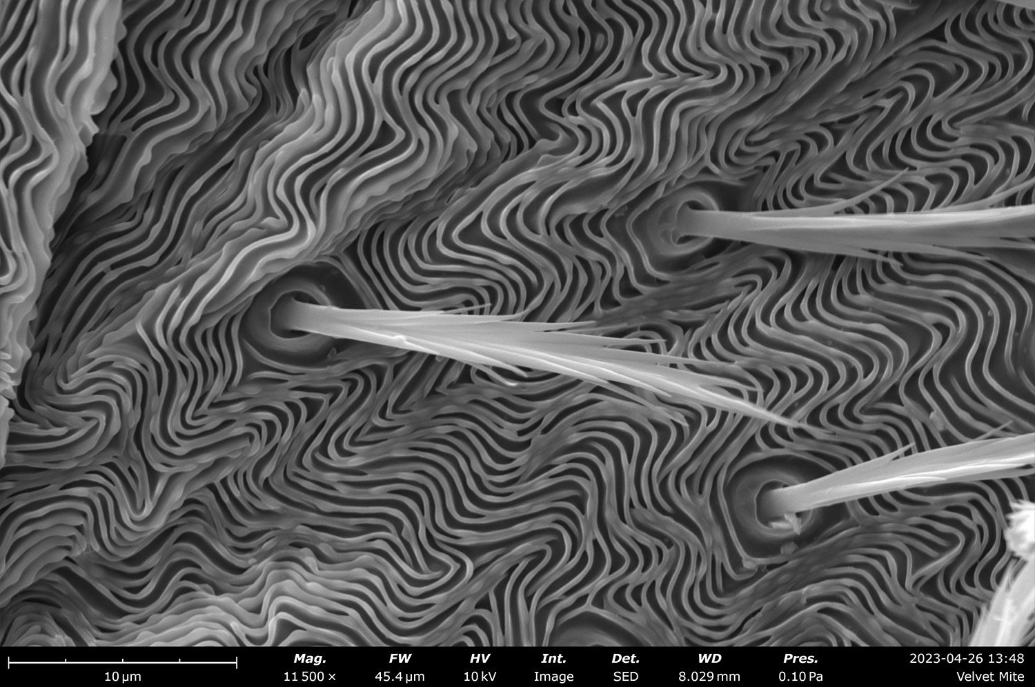
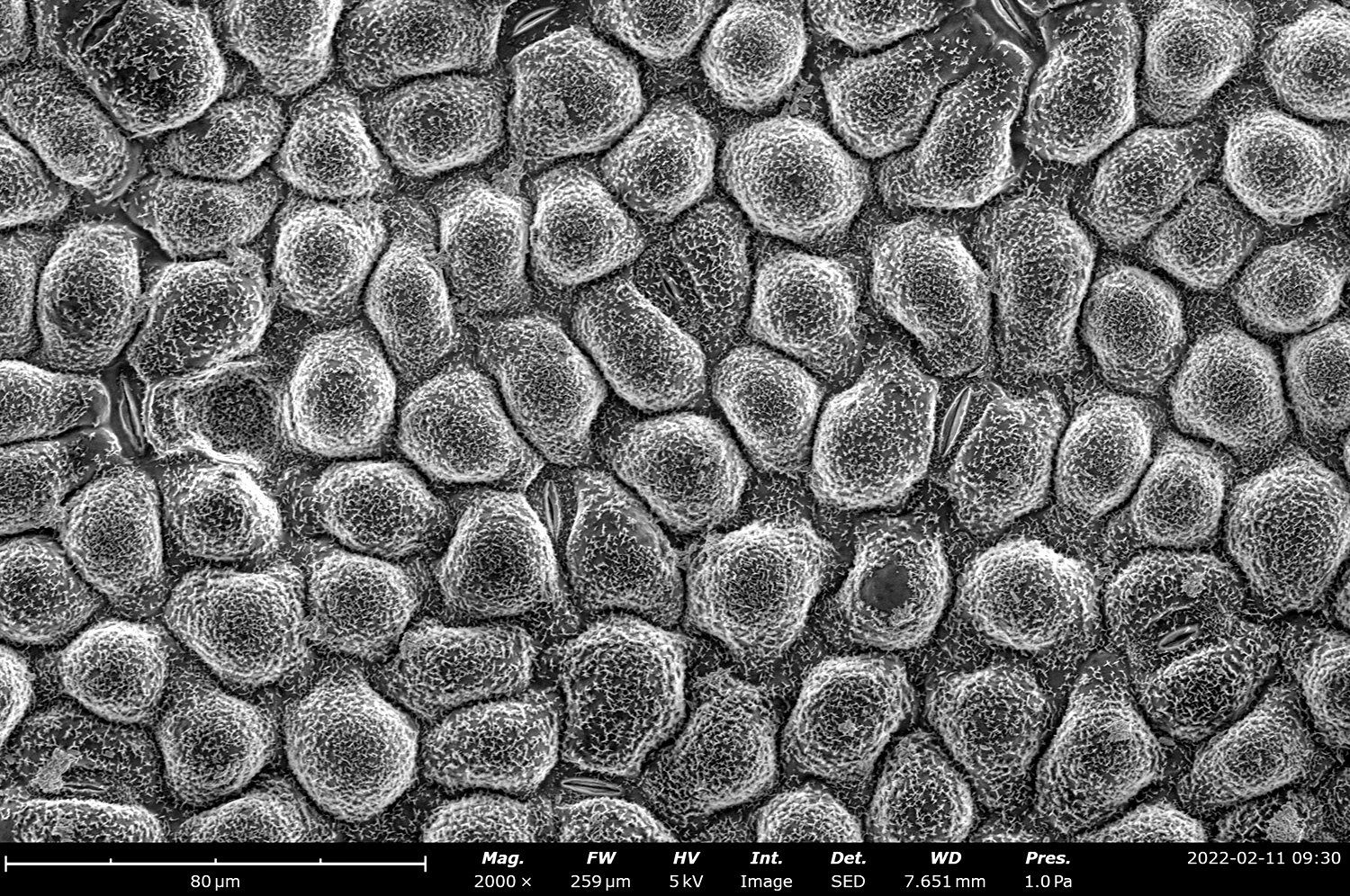
High-brightness electron sources achieve sharp, detailed images with excellent resolution and contrast, making it ideal for a wide range of applications from routine analysis to advanced research.
Longer Lifetime
The lifetime of the CeB6 and FEG sources is about 15 to 100 times longer, respectively, than tungsten and do not fail catastrophically, allowing preventative maintenance to be scheduled in advance.
Versatile Accelerating Voltage Ranges
Adapt to various sample types – whether delicate, beam-sensitive materials or denser metals – by leveraging a broad accelerating voltage range.
Talk to an Instrumentation Specialist Today!
Long-life Electron Sources for Every Application
The Cerium Hexaboride (CeB6) electron source, used in the Phenom XL, Pro/ProX, and Pure models, offers a brighter and longer-lasting beam compared to traditional tungsten sources. This makes it easier to capture high-quality images and EDS data with consistent results. With a significantly longer lifetime and stable emission, the CeB6 source minimizes downtime, and replacements can be easily performed on-site at predictable intervals.
The Field Emission Gun (FEG), exclusively used in the Phenom Pharos, provides unmatched beam brightness and coherence. The Schottky FEG, a field-assisted thermionic emitter, excels in applications requiring nanometer spatial resolution or imaging at low accelerating voltages, making it the go-to choice for advanced research and intricate sample analysis.
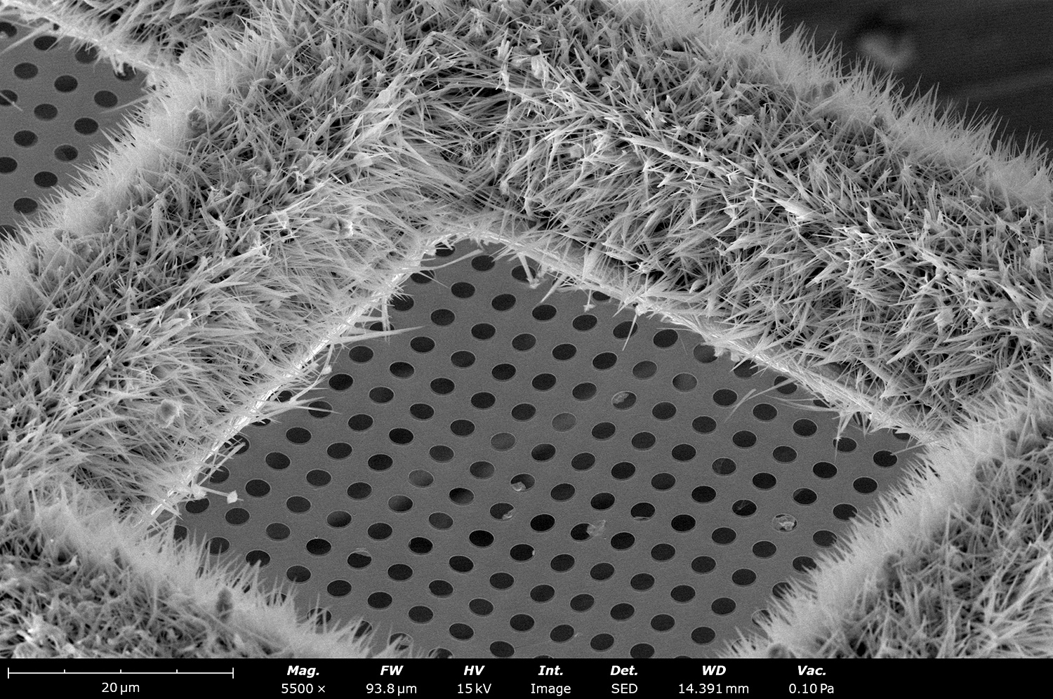
Phenom Electron Sources
Features - CeB6 Source
Superior performance compared to Tungsten
The Phenom thermionic source utilizes a highly polished crystal of cerium hexaboride (CeB6) for thermionic emission. Hexaboride crystals have a lower work function than tungsten, allowing them to emit ten times as many electrons across all accelerating voltages. The brighter beam provides two key advantages: higher signal-to-noise and higher resolution, making them a popular choice for most SEM applications.
Low maintenance
CeB6 sources are significantly more stable than tungsten, and always remain warm and under vacuum, so they only require stigmation adjustments every 3-6 months and last about 10 to 15 times longer before requiring replacement. The source slowly degrades over time and doesn’t suddenly burn out, meaning that replacements can be planned in between sessions and quickly performed on-site.
Reduced energy spread
Electrons emitted from the CeB6 source have a narrower range of energies than those emitted from tungsten, which results in better spectral resolution in energy-dispersive X-ray spectroscopy (EDS) analysis. This allows for more accurate analysis of the sample’s elemental composition. The narrow energy spread also improves imaging resolution compared to tungsten sources.
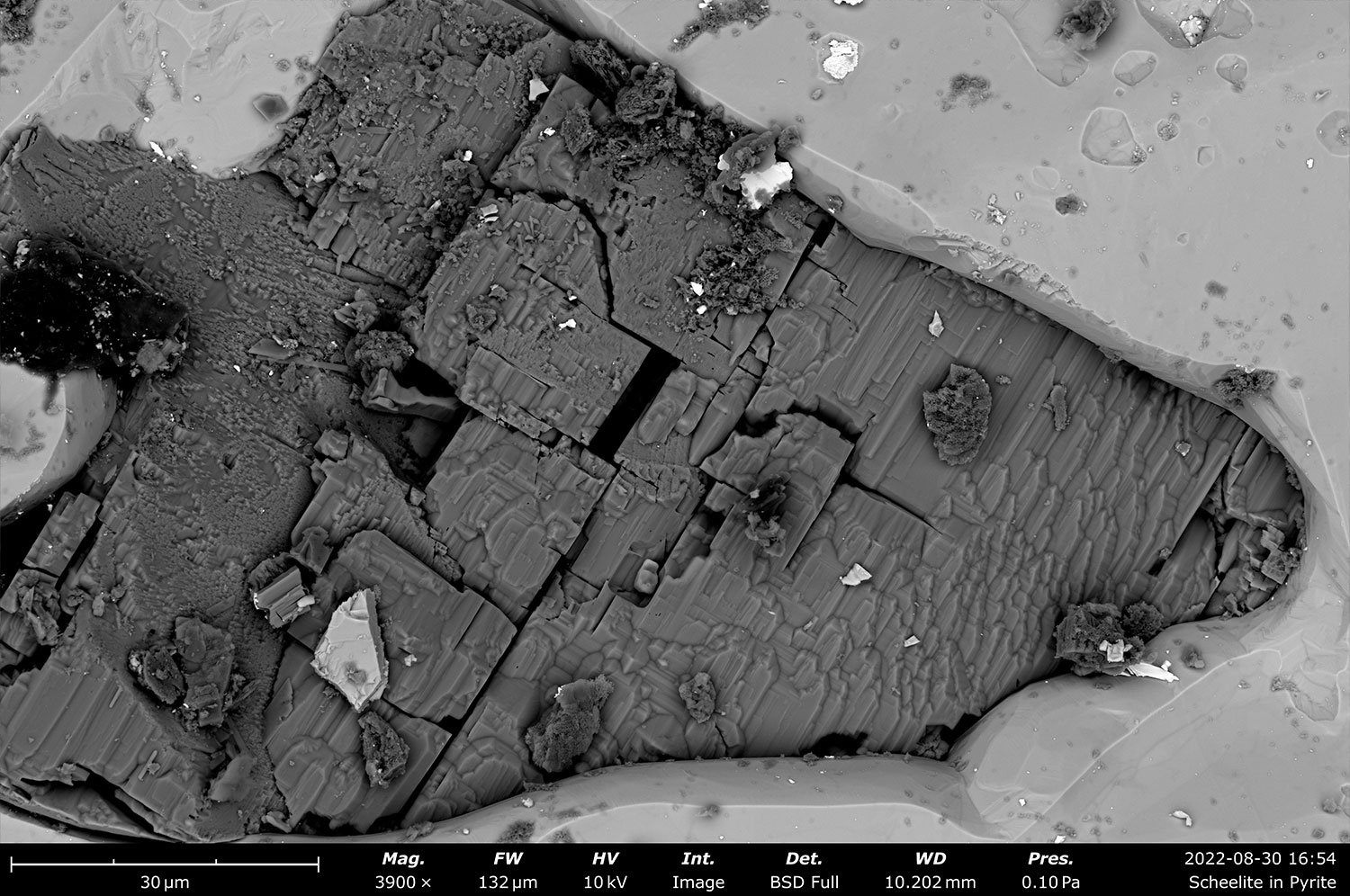
Phenom Electron Sources
Features – FEG Source
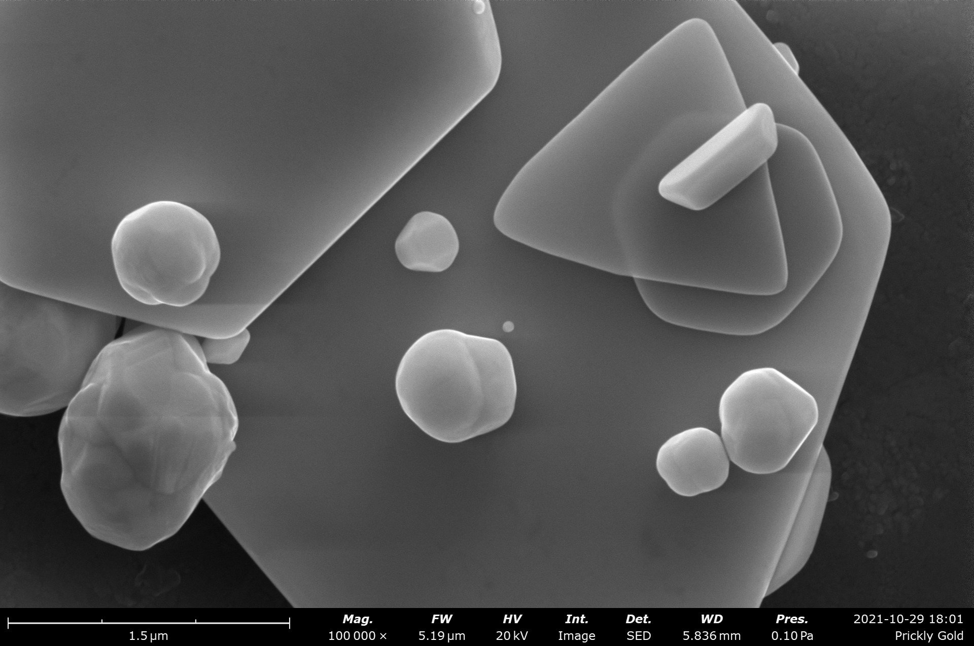
Field-emission performance for everyone
The FEG source in the Phenom Pharos effortlessly delivers results that are traditionally expected from advanced floor-model systems. Only FEG sources can provide the most coherent and bright beam of electrons which allows it to excel at analysis or low-kV imaging.
Low voltage imaging
Because field emission sources are brighter, they can efficiently emit electrons even at low accelerating voltages. This gives FE-SEMs the unique ability to support low-kV imaging, which refers to acquiring SEM images at an accelerating voltage of less than 5 kV.
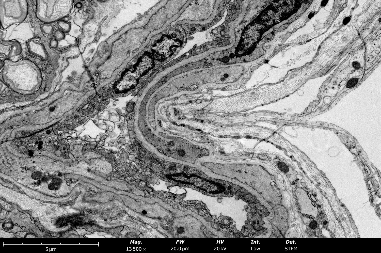
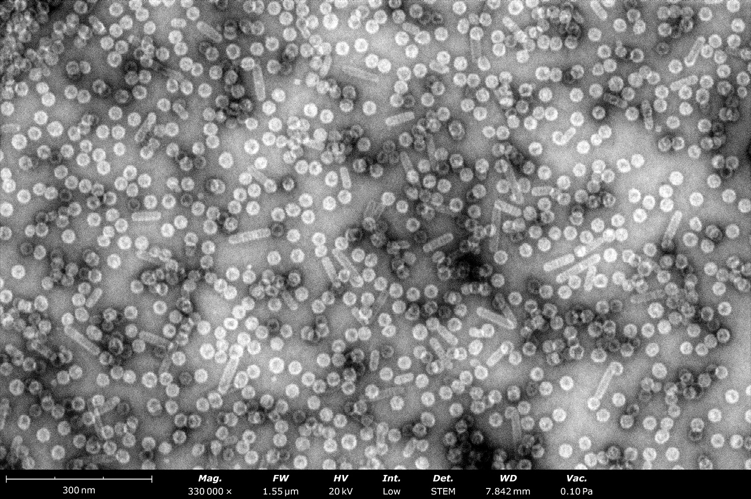
STEM-in-SEM
The advanced capabilities of the FEG source in the Phenom Pharos provide the added possibility of transmission imaging. STEM-in-SEM mode involves acquiring high-resolution images of a sample’s interior structure by analyzing the transmitted electrons that are emitted beneath the sample. The technique is suitable for imaging electron-transparent samples (typically < 100 nm in thickness) such as tissue sections or nanoparticles.
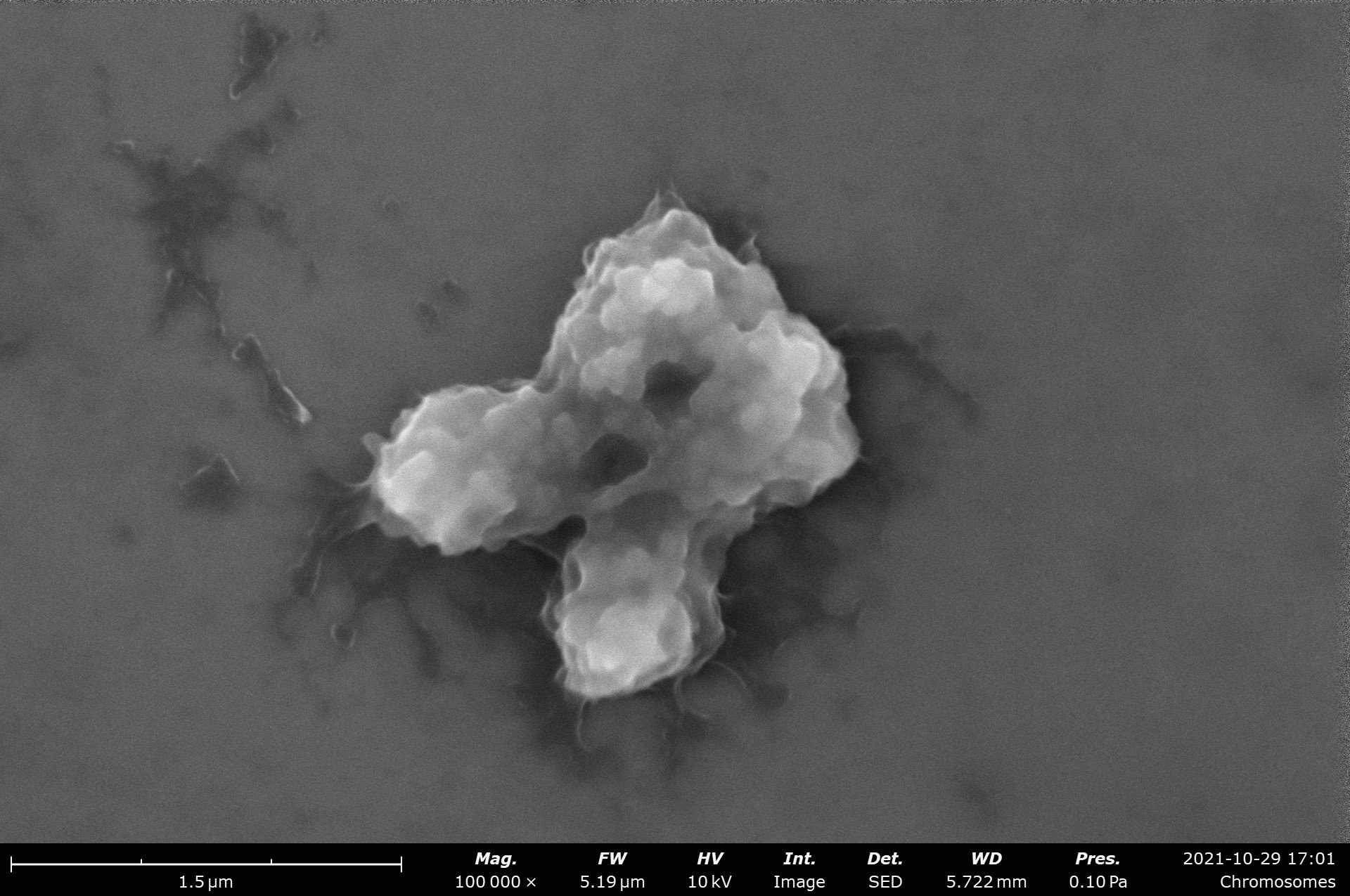
Phenom Electron Sources
Product Knowledgebase
Webinar
Using Automated SEM/EDS Analysis to Enhance Parts Cleanliness
Maintaining technical cleanliness is critical in industries where contamination can compro…
Blog
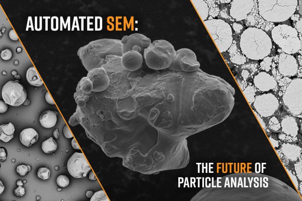
Automated SEM: The Future of Particle Analysis
Particle analysis involves characterizing the size, morphology, and composition of powders…
White Paper
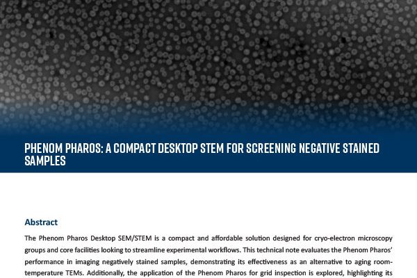
Phenom Pharos: A Compact Desktop STEM for Screening Negative Stained Samples
The Phenom Pharos Desktop SEM/STEM is a compact and affordable solution designed for cryo-…