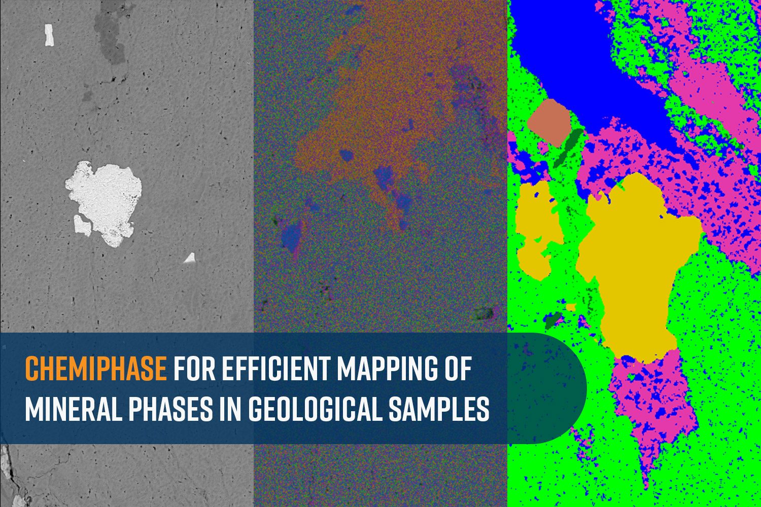
Geological samples are complex matrices of minerals, each with their own unique compositions and structures. Phase identification, in a general sense, is the process of…
Posted: September 4, 2024 | Technology: Scanning Electron Microscopy
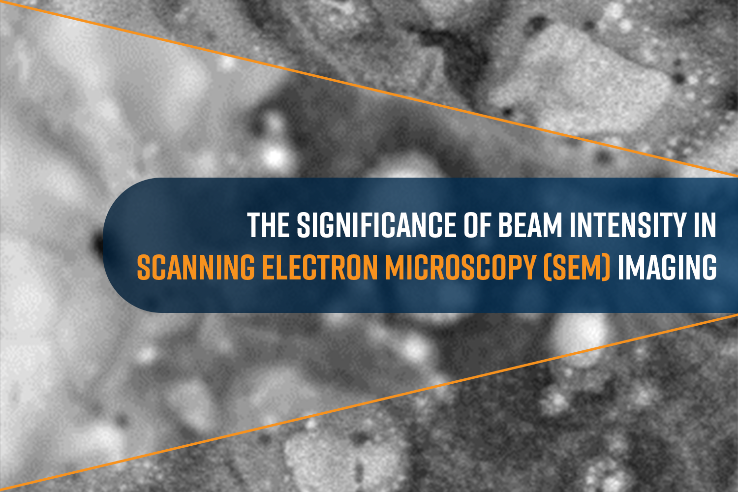
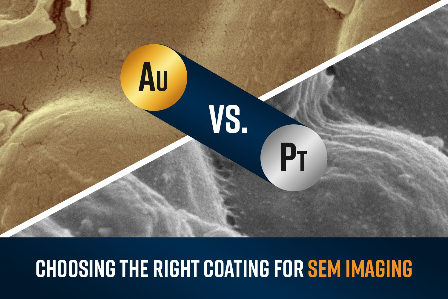
Scanning Electron Microscopy (SEM) is an indispensable tool in various scientific and industrial fields, providing high-resolution images of sample surfaces. Among the numerous parameters that…
Posted: August 21, 2024 | Technology: Scanning Electron Microscopy
In a scanning electron microscope (SEM) with Energy Dispersive X-ray Spectroscopy (EDS), a sample’s elemental composition is identified via the X-rays emitted during the electron…
Posted: July 24, 2024 | Technology: Scanning Electron Microscopy

Energy Dispersive X-ray Spectroscopy (EDS) is an analytical technique used for elemental analysis and chemical characterization of materials. By detecting and measuring the energy of…
Posted: July 17, 2024 | Technology: Scanning Electron Microscopy
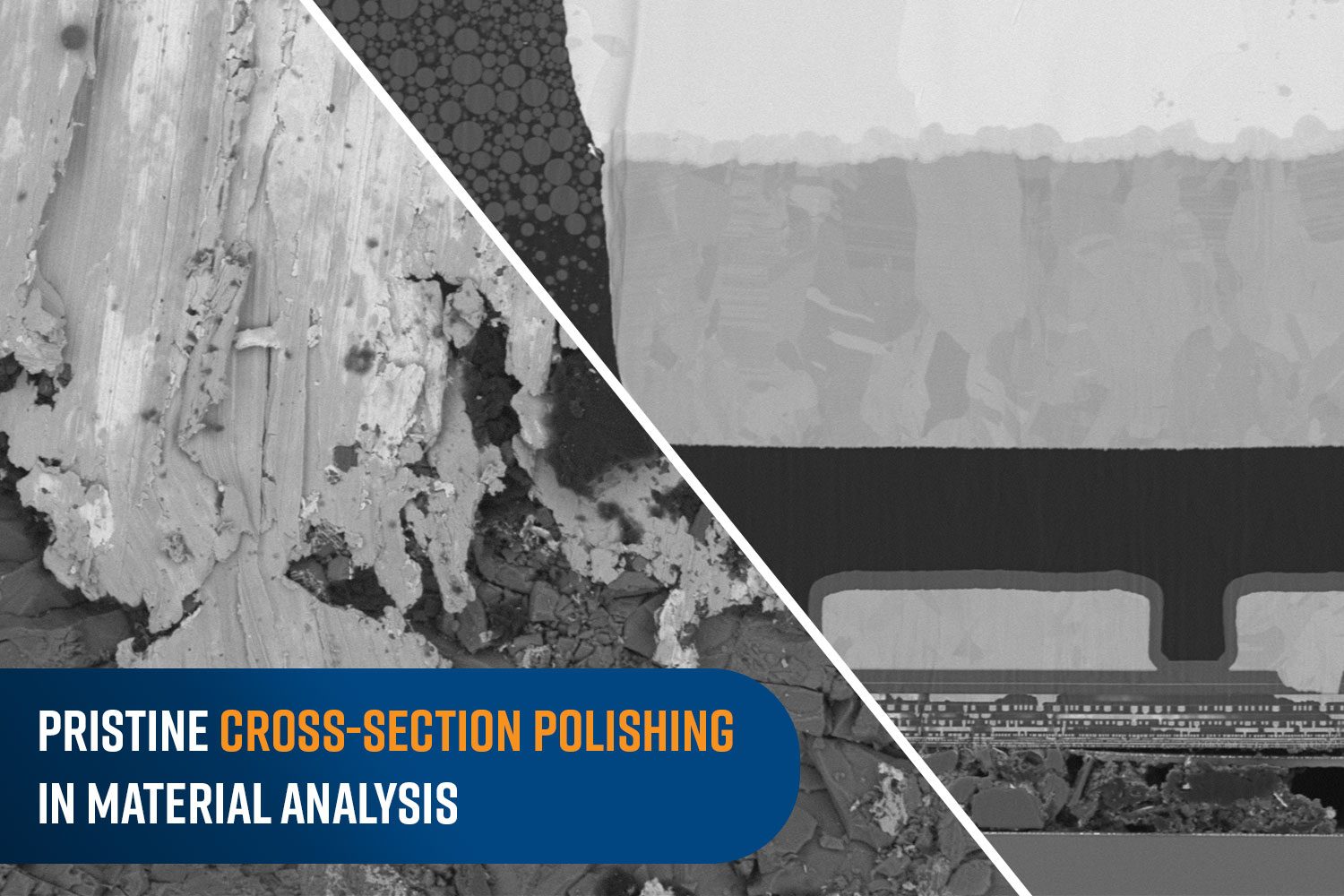
In material science, cross-section polishing is a critical method to enable the detailed examination of a sample material’s microstructure. This technique is essential for understanding…
Posted: July 10, 2024 | Technology: Scanning Electron Microscopy
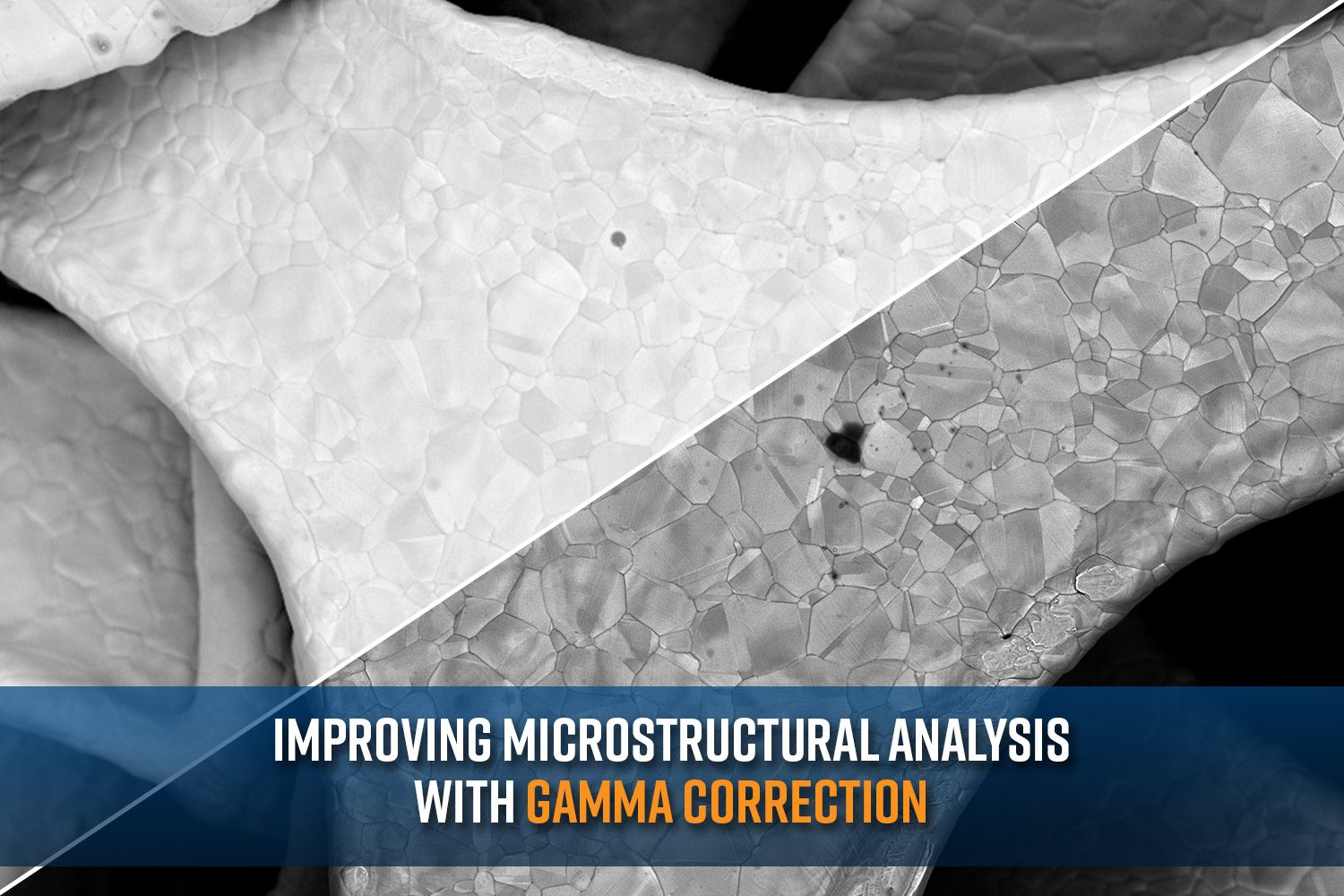
Scanning Electron Microscopy (SEM) is one of the most important tools in the arsenal of modern material science used to characterize micro and nanoscale features….
Posted: June 19, 2024 | Technology: Scanning Electron Microscopy
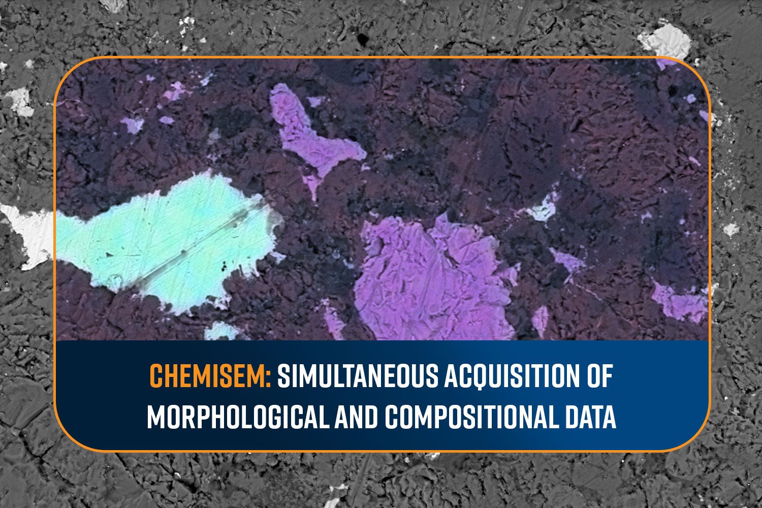
A scanning electron microscope (SEM) is capable of visualizing compositional heterogeneity on the surface of a sample by employing a backscattered electron detector (BSD). A…
Posted: May 22, 2024 | Technology: Scanning Electron Microscopy
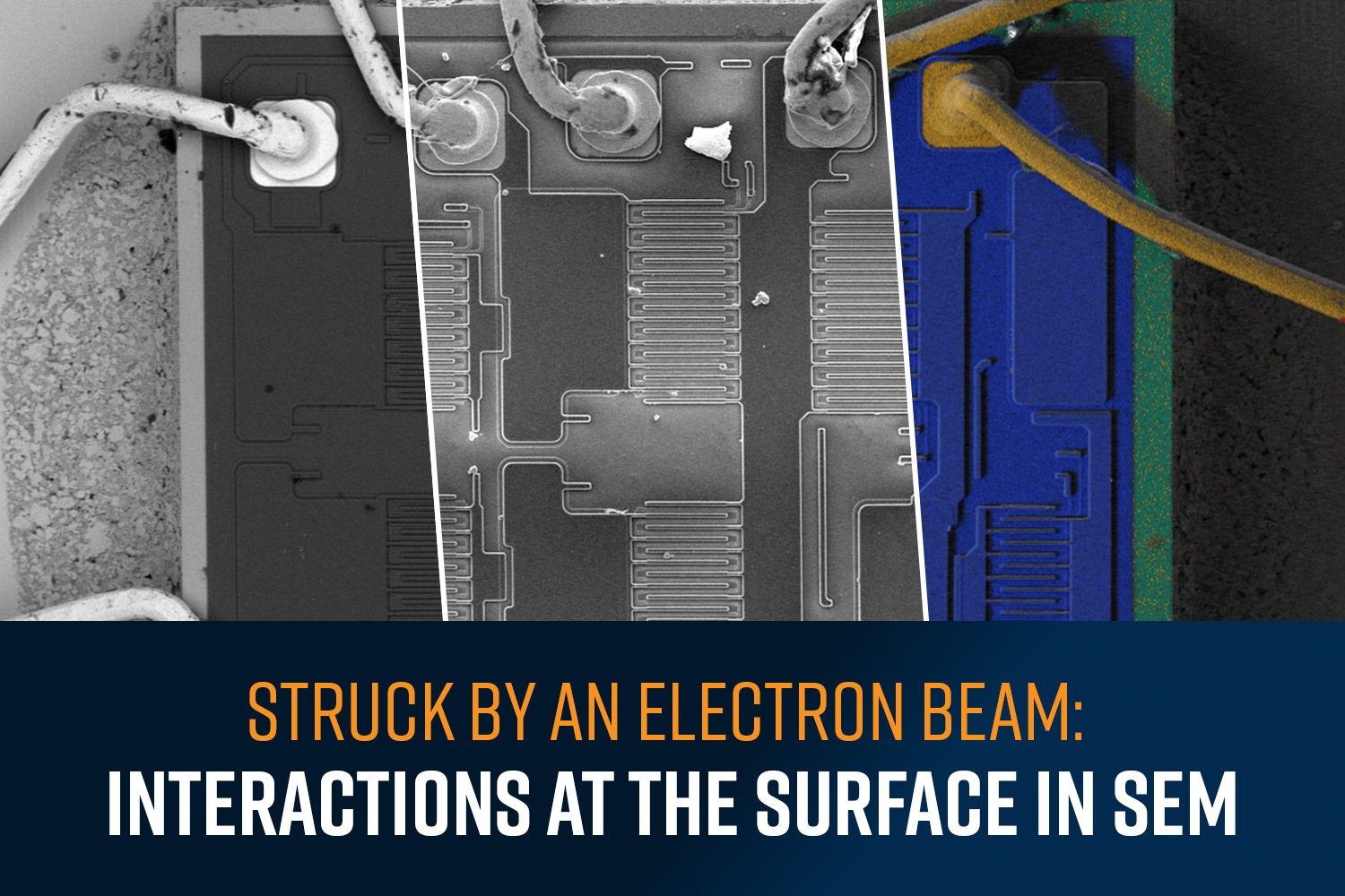
Scanning Electron Microscopy (SEM) generates high-resolution images by scanning a focused beam of electrons across the sample surface and detecting the signals produced through beam-sample…
Posted: May 8, 2024 | Technology: Scanning Electron Microscopy

Technical cleanliness is an analytical standard to determine the level of particulate contamination on machined parts. The goal of technical cleanliness is to characterize the…
Posted: May 2, 2024 | Technology: Scanning Electron Microscopy
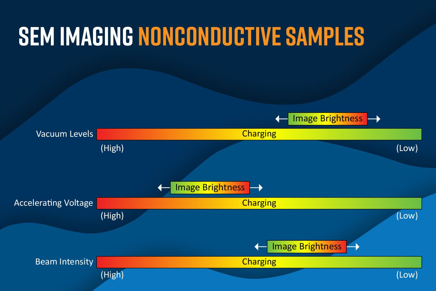
Charging is one of the most common issues when imaging non-conductive samples by scanning electron microscope (SEM) as it can distort images and damage the…
Posted: April 24, 2024 | Technology: Scanning Electron Microscopy
One of the most common challenges when analyzing non-conductive samples with a scanning electron microscope (SEM) is the charging effect. Without a conductive path, the…
Posted: April 18, 2024 | Technology: Scanning Electron Microscopy

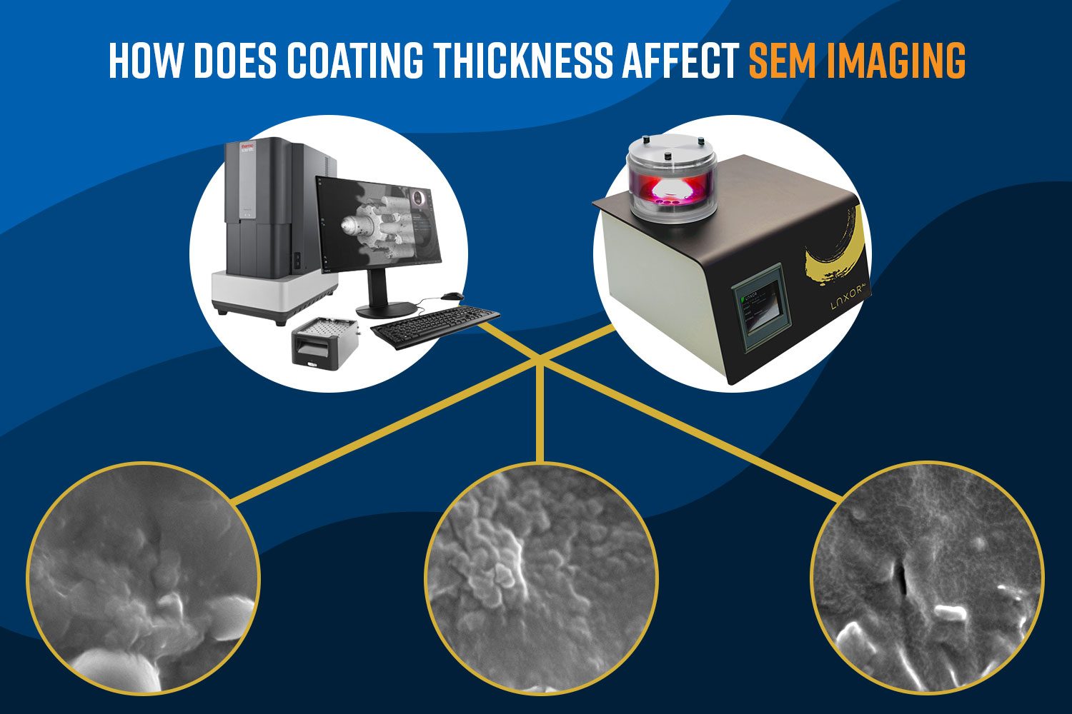
Integrating the ability to perform high-resolution imaging and compositional analysis of materials into any laboratory becomes simplified with a desktop scanning electron microscope (SEM). In…
Posted: April 10, 2024 | Technology: Scanning Electron Microscopy